Microcosmic area charge injecting and quantitative analysis method in nanometer silicon floating gate structure

A technology of charge injection and nano-silicon, applied in measuring devices, scanning probe microscopy, instruments, etc., to achieve high detection resolution and good repeatability

Active Publication Date: 2014-01-15
NANJING UNIV
View PDF6 Cites 4 Cited by
  • Summary
  • Abstract
  • Description
  • Claims
  • Application Information

AI Technical Summary

Problems solved by technology

However, in the existing research work, the surface potential signal is only used as an indirect information of the injected charge, and there is a lack of analysis of the quantitative relationship between the surface potential and the number of injected charges.

Method used


Image

  • Microcosmic area charge injecting and quantitative analysis method in nanometer silicon floating gate structure
  • Microcosmic area charge injecting and quantitative analysis method in nanometer silicon floating gate structure
  • Microcosmic area charge injecting and quantitative analysis method in nanometer silicon floating gate structure

Examples


Embodiment Construction

[0030] (1) Injection of microscopic regional charges in the nano-silicon floating gate structure

[0031] 1. Preparation of samples with nano-silicon floating gate structure

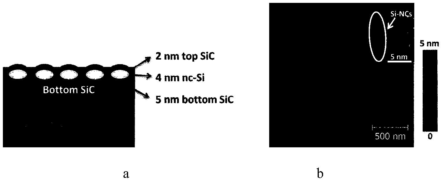
[0032] The nano-silicon floating gate structure sample is a silicon carbide / nano-silicon / silicon carbide (SiC / nc-Si / SiC) sandwich structure on a p-type single crystal silicon substrate (resistivity 1.5–3Ωcm), in which the thickness of the underlying silicon carbide is 5nm, the thickness of the nano-silicon layer is 4nm, and the top layer of silicon carbide is 2nm. For the charge injection test, the sample substrate was bonded to the test tray using conductive silver paste (Silver Paint), and finally the tray and the sample were placed in the operating room of the atomic force microscope.

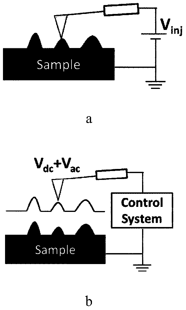
[0033] 2. Charge injection of nano-silicon floating gate structure

[0034] At room temperature and in a clean air atmosphere, let the atomic force microscope (Bruker, Germany, Nanoscope3D model) work in the tapping ...


PUM


Abstract

The invention provides a microcosmic area charge injecting and quantitative analysis method in a nanometer silicon floating gate structure. By means of an atomic force microscope and a Kelvin detection method, charge injecting of the nanometer silicon floating gate structure is achieved. The nanometer silicon floating gate structure is of a silicon carbide structure or a nanometer silicon structure or a silicon carbide sandwich structure. In a tapping mode of the atomic force microscope, a sample silicon substrate additionally exerts bias voltage of positive 3V and negative 3V on a conductive probe of the atomic force microscope, the surface of the nanometer silicon floating gate structure on the sample silicon substrate is scanned, and charge injecting is achieved. After charge injecting, the atomic force microscope is immediately switched to a surface potential mode from the tapping mode, and in the surface potential mode, a surface potential signal of a sample is obtained through two steps of scanning and the Kelvin detection method. The charge injecting is quantitatively researched through static electric field analysis and numerical calculation, and the charge injecting quantity can be obtained through the static electric field analysis and the numerical calculation.

Description

1. Technical field: [0001] The invention proposes a new method for realizing microscopic region charge injection and quantitative detection in a nanometer silicon floating gate structure by using an atomic force microscope (AFM) and a Kelvin probe. 2. Background technology: [0002] The research on the charge injection of nano-silicon at the microscopic level, especially the quantitative research, is an important basis for in-depth understanding of the physical properties of silicon-based materials and improving the state performance of silicon-based devices. However, traditional electrical tests such as C-V tests can only obtain the macroscopic properties of the sample, and cannot further understand its microscopic electrical effects. In recent years, atomic force microscopy and its Kelvin detection extension mode are being increasingly used in the characterization of the morphology and surface potential of semiconductor materials and device microscopic regions, but in the ...

Claims


Application Information

Patent Timeline
Patent Type & Authority Applications(China)
IPC IPC(8): G01Q60/24
Inventor 徐骏许杰李伟张鹏展王越飞徐岭余林蔚陈坤基
Owner NANJING UNIV
Why Eureka
Try Eureka