Wafer transmission system

A chip transmission system and chip technology, applied in the direction of conveyor objects, transportation and packaging, electrical components, etc., can solve the problems of time and cost waste, affecting the production process yield, aging and wear of transmission components, etc.

Inactive Publication Date: 2014-01-15
IND TECH RES INST
View PDF4 Cites 5 Cited by
  • Summary
  • Abstract
  • Description
  • Claims
  • Application Information

AI Technical Summary

Problems solved by technology

[0004] In addition, after a long-term use of the wafer transfer system, the materials of the above-mentioned transmission components are aging and worn more and more seriously. Therefore, when the machine has been running for a period of time, it must be shut down to replace the aging and worn components, resulting in time and cost. Waste, affecting production process yield

Method used


Image

  • Wafer transmission system
  • Wafer transmission system
  • Wafer transmission system

Examples


Embodiment Construction

[0051] The possible implementation of the wafer transfer system of the present invention will be described below through the embodiments and accompanying drawings.

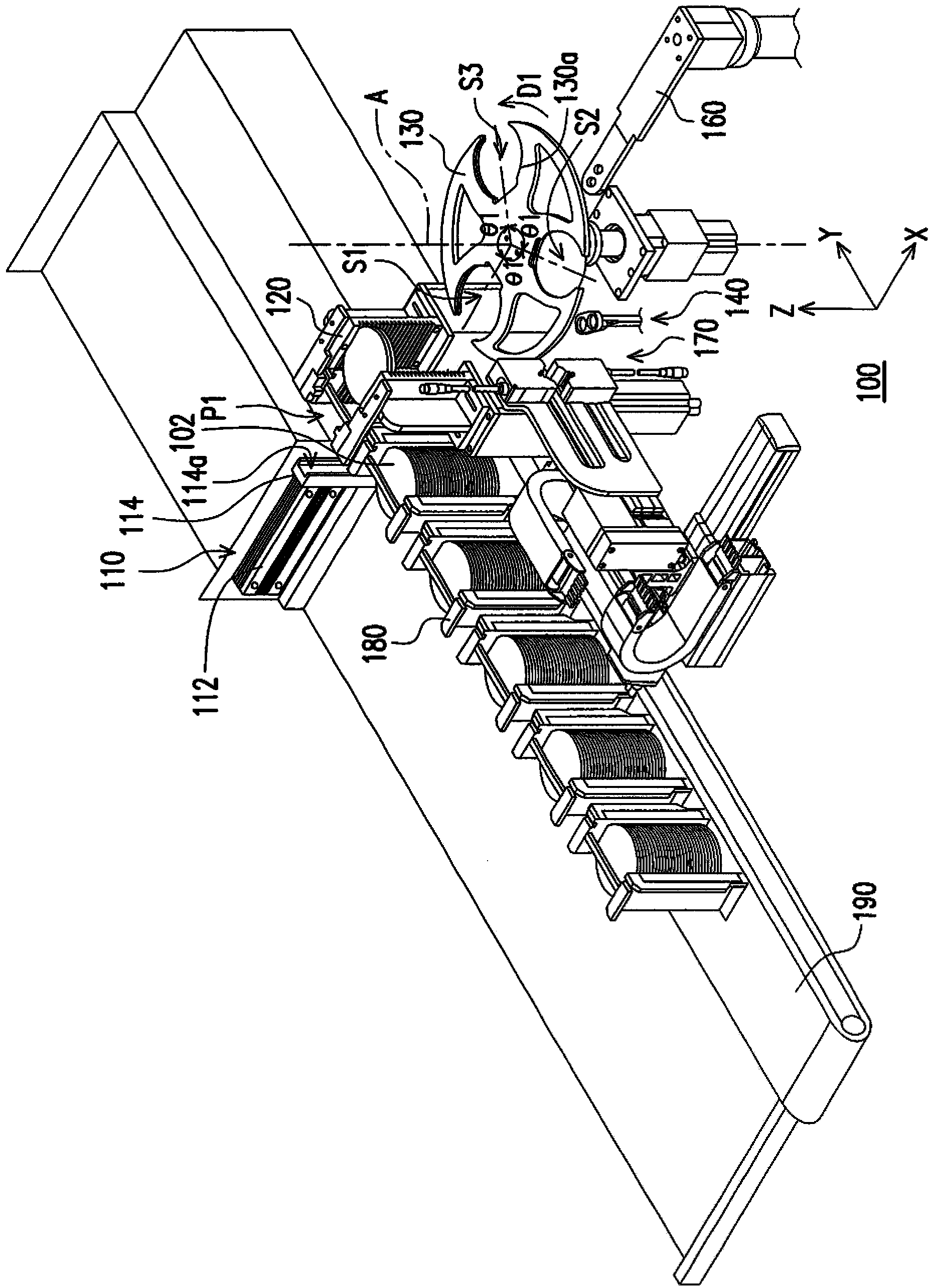
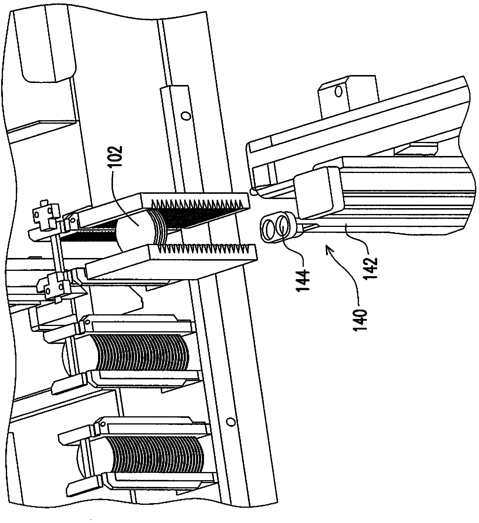
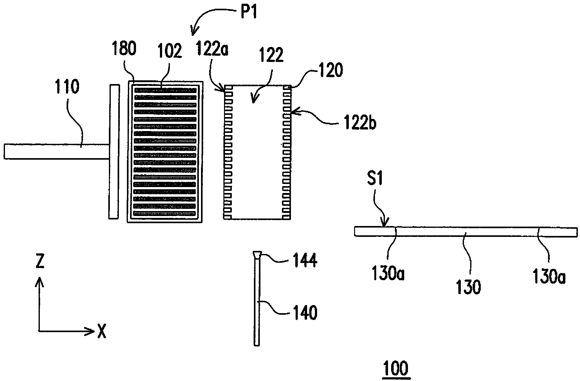
[0052] figure 1 A wafer transfer system 100 according to an embodiment of the present invention is shown. figure 2 This is a partially enlarged view of the wafer transport system 100 . The wafer transfer system 100 of this embodiment includes a feeding mechanism 110 , a positioning jig 120 , a carrying unit 130 and a pick-and-place unit 140 . figure 2 The enlarged view of FIG. 2 omits the carrying unit 130 to clearly show the pick-and-place unit 140 located below the carrying unit 130 .

[0053] The wafer transfer system 100 of the present embodiment can be applied in semiconductor manufacturing process to transfer the wafer 102 between various manufacturing process reaction chambers. Usually, the wafers 102 are stored in the wafer cassette 180, and the wafers 102 are taken out from the wafer cassette 180 by ...


PUM


Abstract

The invention discloses a wafer transmission system suitable for transmitting a plurality of wafers from one wafer box. The wafer transmission system comprises a positioning tool, a feeding mechanism, a bearing unit and a removing unit. The positioning tool is provided with a plurality of containing grooves corresponding to the wafers; the feeding mechanism is suitable for simultaneously loading the wafers from the wafer box into the containing grooves of the positioning tool along a first direction of a surface. The bearing unit comprises a rotary disk provided with a plurality of bearing portions. The rotary disk is suitable for rotating around an axial direction of a vertical surface, so the bearing portions can pass a releasing position in sequence, wherein the projections of the releasing position and the positioning tool on the plane are arranged in the first direction. The removing unit is used for respectively transmitting the wafers in the positioning tool to the bearing portion in the releasing position in sequence.

Description

technical field [0001] The invention relates to a wafer transfer system. Background technique [0002] With the increasing integration of semiconductor elements of integrated circuits, the accuracy and production efficiency of the manufacturing process are relatively important. Slight errors in the semiconductor manufacturing process may lead to the failure of the manufacturing process, resulting in damage to the wafer, thus costing a lot of money. [0003] However, the structure and motion of the known wafer transfer system are quite complicated, and the mechanical arm including rods and bearings must perform actions such as rotation, extension, and retraction to transfer the wafer to the position, thus limiting the production efficiency. However, the frequent use of the mechanical arm will often cause the material of the transmission element to age, wear and even deform, resulting in the generation of material particles and dust falling, becoming a source of pollution. D...

Claims


Application Information

Patent Timeline
Patent Type & Authority Applications(China)
IPC IPC(8): H01L21/677H01L21/68
CPCH01L21/67766H01L21/67781H01L21/68
Inventor 罗传仙陈钧贺廖俊杰
Owner IND TECH RES INST
Why Eureka
Try Eureka