Display panel, manufacture method thereof, display device

A technology for a display panel and a manufacturing method, which is applied in the fields of display devices, display panels and their manufacturing, and can solve problems such as complex optimization schemes, difficult implementation, and complex technical means, and achieve the effects of reducing brightness, improving contrast, and reducing light leakage

Active Publication Date: 2014-01-22
BOE TECH GRP CO LTD
View PDF4 Cites 23 Cited by
  • Summary
  • Abstract
  • Description
  • Claims
  • Application Information

AI Technical Summary

Problems solved by technology

[0005] However, in terms of increasing the maximum brightness, increasing the aperture ratio can only increase the maximum brightness of the display device within a certain range. More importantly, some new process and design problems will arise in the process of increasing the aperture ratio; On the one hand, when optimizing the Cell process, the optimization schemes adopted are relatively complicated
To sum up, the technical means used in the prior art to improve the contrast of the display device are relatively complicated and not easy to implement.

Method used


Image

  • Display panel, manufacture method thereof, display device
  • Display panel, manufacture method thereof, display device
  • Display panel, manufacture method thereof, display device

Examples


Embodiment 1

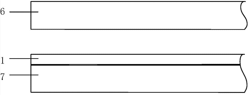
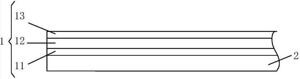
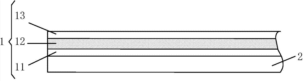
[0038] figure 1 It is a schematic structural diagram of a display panel provided in Embodiment 1 of the present invention, Figure 2a for figure 1 Schematic diagram of the structure of the box substrate in ; Figure 2b for Figure 2a The schematic diagram of the electrochromic structure on the cell substrate absorbing light leakage is shown; as figure 1 , 2a As shown in and 2b, the display panel includes an array substrate 6, an opposite cell substrate 7 and an electrochromic structure 1, and the electrochromic structure 1 is used to absorb light leakage from the display panel when the display panel is in a dark state.

[0039] It should be noted that the electrochromic structure 1 includes: an electrochromic layer 12, a first transparent electrode 11 and a second transparent electrode 13, the electrochromic layer 12 is located between the first transparent electrode 11 and the second transparent electrode 13, Optionally, the materials of the first transparent electrode 1...

Embodiment 2

[0049] image 3 A schematic structural diagram of the display panel provided in Embodiment 2 of the present invention, as shown in image 3 As shown, the display panel includes: an array substrate 6 and a box substrate. The electrochromic structure 1 is located on the box substrate. Specifically, the electrochromic structure 1 is located on the front side of the first substrate substrate 2. On the first substrate The front of the substrate 2 is also provided with a color filter 3, the color filter 3 includes: a color matrix pattern 31 and a black matrix 32, the black matrix 32 defines a pixel area, the color matrix pattern 31 is formed in the pixel area, and the electrochromic structure 1 is formed in on the color film.

[0050] It should be noted that the difference between this embodiment and the first embodiment is that the electrochromic structure 1 is formed on the color filter 3 in this embodiment. However, no matter whether the electrochromic structure 1 is formed dir...

Embodiment 3

[0059] Embodiment 3 of the present invention provides a display device. The display device includes: a display panel. The display panel adopts the display panel in Embodiment 1 or Embodiment 2 above. For details, please refer to Embodiment 1 and Embodiment 2 above. Here No longer.

[0060] The display device may be any product or component with a display function such as a mobile phone, a tablet computer, a television, a monitor, a notebook computer, a digital photo frame, a navigator, and the like.

[0061] Embodiment 3 of the present invention provides a display device. The display device includes a display panel, wherein an electrochromic structure is formed on the display panel. When the display panel is in a bright state, the electrochromic structure is in a transparent state; when the display panel In the dark state, the electrochromic structure is in a colored state, and the electrochromic structure in the colored state can absorb light, thereby minimizing the light lea...


PUM


Abstract

The invention discloses a display panel, a manufacture method thereof and a display device. The display panel comprises an array substrate and a pair box substrate. The display panel further comprises an electrically induced discoloration structure. The electrically induced discoloration structure is used for absorbing leaked light of the display panel when the display panel is in a dark state. When the display panel is in a bright state, the electrically induced discoloration structure is in a transparent state. When the display panel is in a dark state, the electrically induced discoloration structure is in a coloring state. The electrically induced discoloration structure can absorb light when being in the coloring state so as to reduce the leaked light of the display panel in the dark state to a largest degree, so that the smallest luminance of the display panel is reduced, consequently, the contrast ratio of the display panel is effectively improved.

Description

technical field [0001] The present invention relates to the field of display technology, in particular to a display panel, a manufacturing method thereof, and a display device. Background technique [0002] With the development of science and technology and the progress of society, liquid crystal displays have been more and more widely used by people, and play a vital role in industrial production and people's lives. At present, high-quality liquid crystal displays are more and more favored by people. Many companies in the field of display technology have invested huge manpower and material resources in the directions of high contrast, fast response, and low power consumption. [0003] The contrast ratio of a liquid crystal display refers to the ratio of the maximum brightness to the minimum brightness of the liquid crystal display device during the display process. Therefore, the contrast ratio of the liquid crystal display device is not only related to the maximum bright...

Claims


Application Information

Patent Timeline
Patent Type & Authority Applications(China)
IPC IPC(8): G02F1/153G02F1/1333
CPCG02F1/153G02F1/133512G02F2001/1635G02F1/133357G02F1/1333G02F1/157G02F1/163G03F7/0007
Inventor 石岳柳在健
Owner BOE TECH GRP CO LTD
Why Eureka
Try Eureka