Alignment method for internal layers in direct writing type photoetching system

A lithography system and direct-writing technology, which is applied in microlithography exposure equipment, optics, photoplate-making process of pattern surface, etc., can solve the problem that the front and back of the circuit board cannot be accurately aligned, and achieve exposure saving time, ensuring alignment accuracy, and simple calculation

Inactive Publication Date: 2014-01-22
TIANJIN JINXIN MICROELECTRONICS TECH CO LTD
View PDF5 Cites 22 Cited by
  • Summary
  • Abstract
  • Description
  • Claims
  • Application Information

AI Technical Summary

Problems solved by technology

[0005] The object of the present invention is to provide a method for aligning inner layers in a direct-writing lithography system, so as to solve the problems in the front and ba...

Method used


Image

  • Alignment method for internal layers in direct writing type photoetching system
  • Alignment method for internal layers in direct writing type photoetching system
  • Alignment method for internal layers in direct writing type photoetching system

Examples


Embodiment Construction

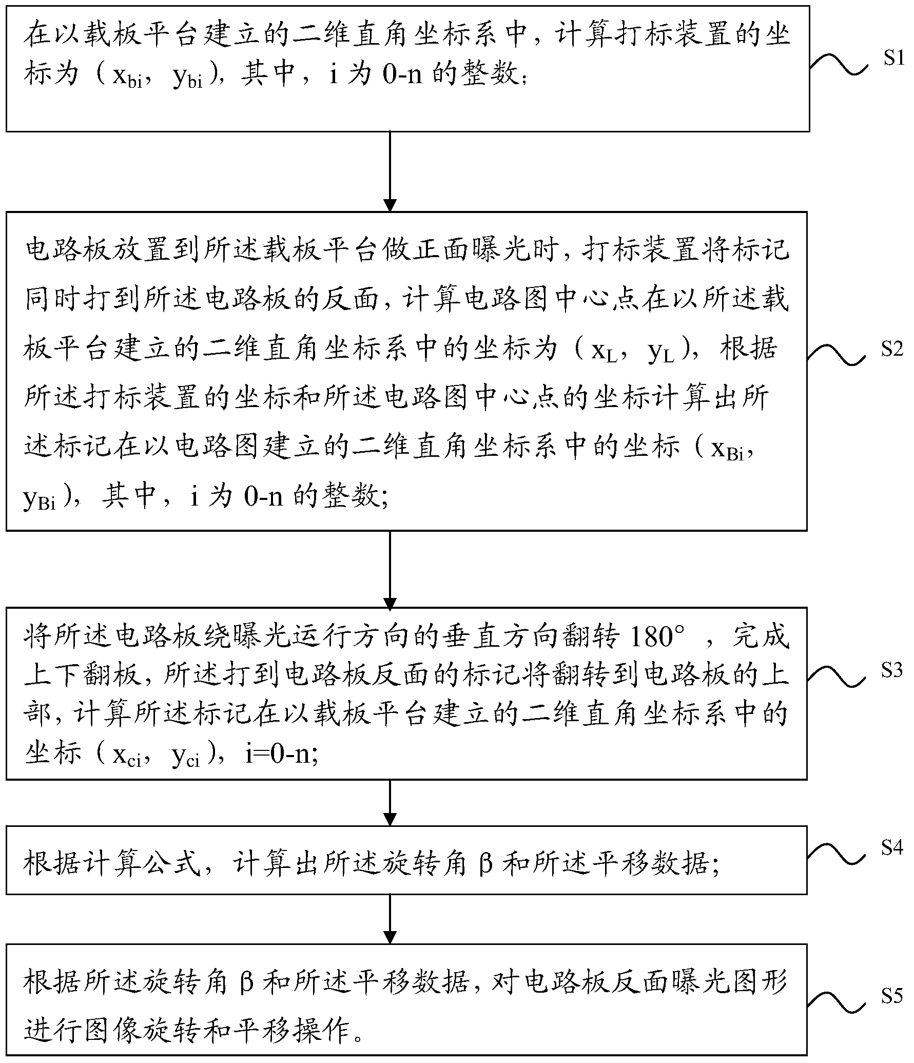
[0021] In order to make the objectives, technical solutions, and beneficial effects of the present invention clearer and clearer, the present invention will be further described in detail below in conjunction with embodiments. It should be understood that the specific embodiments described herein are only used to explain the present invention and not used to limit the protection scope of the present invention.

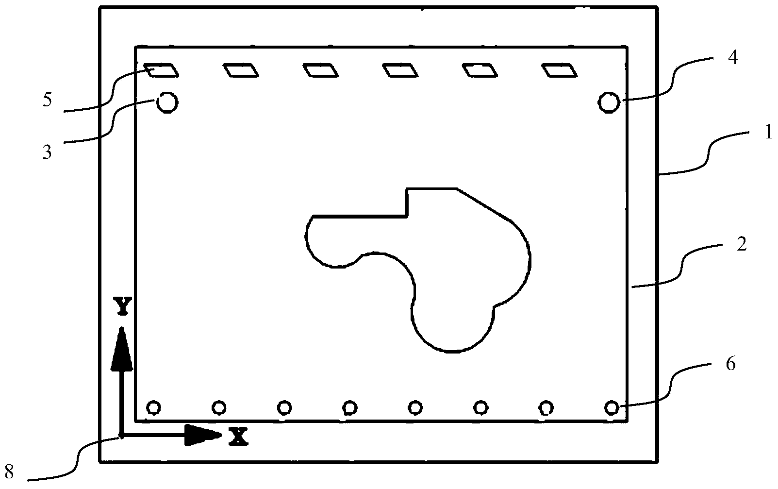
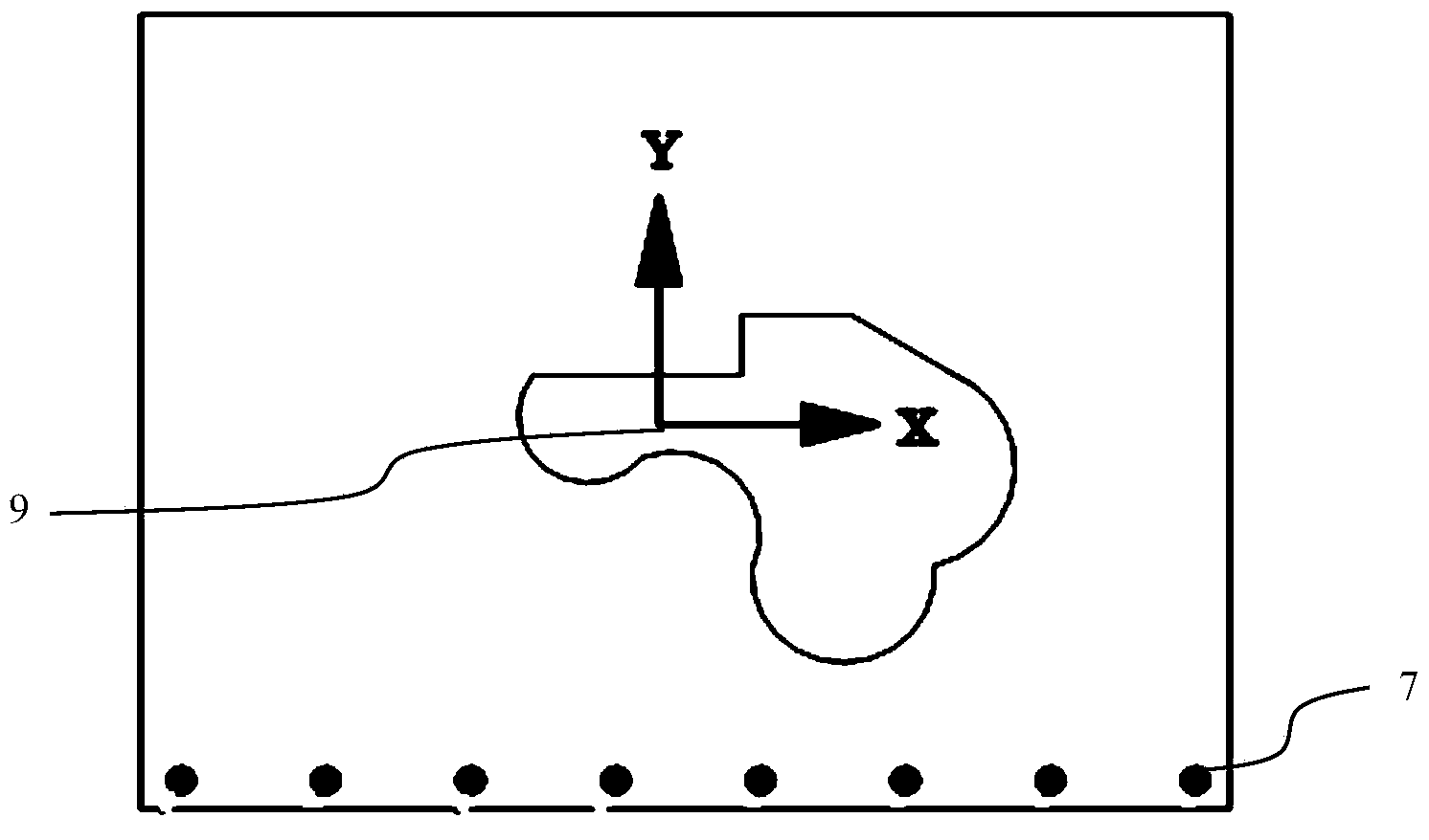
[0022] The working principle of the present invention is: when exposing the front circuit diagram of the circuit board in the direct writing lithography system, the marking device simultaneously marks the mark on the reverse side of the circuit board, marking the blank part on the lower frame of the circuit board, and at the same time The position data of the mark relative to the carrier platform coordinate system (x bi , Y bi ), i=0-n, where n can be 7, converted to the coordinate system of the circuit diagram, that is (x Bi , Y Bi ), i=0-n, the coordinate system of the...


PUM


Abstract

The invention discloses an alignment method for internal layers in a direct writing type photoetching system. According to the method, during exposure of a front circuit diagram of a circuit board, a marking apparatus leaves marks on the back surface of the circuit board at same time, the marks are left at blank positions on the lower frame of the circuit board, and the position data (x[bi], y[bi]) of the marks relative to the coordinate system of a carrier platform are transformed into the coordinate system of the circuit board to obtain the coordinate (x[Bi], y[Bi]), wherein i is in range of 0 to n and n may be 7 in the position data (x[bi], y[bi]), i is in range of 0 to n in the coordinate (x[Bi], y[Bi]), the center of the circuit board has to be the datum of the coordinate system of the circuit board, and the circuit diagram overturns around a direction perpendicular to an exposure operation direction during exposure of the back surface, i.e., up-and-down overturning; the position data (x[bi], y[bi]) of the marks relative to the coordinate system of the carrier platform are measured, recorded and stored in advance by area array CCD in the system; after up-and-down overturning, exposure of the back surface of the circuit board is carried out, the area array CCD in the system is also used for measuring the position coordinate (x[ci], y[ci]) of the marks, wherein i is in range of 0 to n, the position coordinate (x[ci], y[ci]) and the transformed coordinate (x[Bi], y[Bi]) of the marks in the circuit diagram are analyzed, and rotation and translation data of the circuit diagram are calculated, wherein the angle of rotation is calculated before calculation of the translation data during calculation.

Description

Technical field [0001] The invention belongs to the technical field of printed circuit board lithography, and in particular relates to a method for alignment of inner layers in a direct-write lithography system. Background technique [0002] In the printed circuit board industry, it involves the use of photolithography to make inner circuit boards. For example, the mobile phone circuit board mainly consists of 8 layers of printed circuit board (PCB) circuits, with a line width of less than 4mil (1mil=25.4um), of which 6 layers are inner PCB circuit boards, and 3 of the circuit boards are exposed to the front and back. engraved. During the processing, the front and back circuits of each inner circuit board need to be aligned to ensure that all the vias can correctly connect the front and back lines, otherwise it will be a waste board that will cause short-circuit, open circuit and other problems, and Problem board that will interfere with the front and back lines. [0003] In the...

Claims


Application Information

Patent Timeline
IPC IPC(8): G03F7/20G03F9/00
Inventor 陈勇李显杰
Owner TIANJIN JINXIN MICROELECTRONICS TECH CO LTD
Why Eureka
Try Eureka