Wafer assembly system

An assembly system and wafer technology, applied in transportation and packaging, conveyor objects, electrical components, etc., can solve the problems of low assembly efficiency, high work intensity, high product defect rate, and achieve the effect of positioning and high-precision positioning

Active Publication Date: 2014-01-22
SICHUAN BLUE COLOR ELECTRONICS TECH
View PDF6 Cites 2 Cited by
  • Summary
  • Abstract
  • Description
  • Claims
  • Application Information

AI Technical Summary

Problems solved by technology

However, current diode manufacturers mainly do it manually when welding diode wafers, which has high work intensity, high defect rate and low assembly efficiency.

Method used


Image

  • Wafer assembly system

Examples


Embodiment Construction

[0021] The technical solution of the present invention will be further described in detail below in conjunction with the accompanying drawings, but the protection scope of the present invention is not limited to the following description.

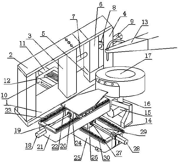
[0022] Such as figure 1 As shown, the wafer assembly system includes a lead wire longitudinal translation assembly, a lead wire lateral translation assembly, a worktable movement assembly, a wafer tray positioning assembly, a wafer tray X-axis translation assembly, a wafer tray Y-axis translation assembly and a wafer loading and unloading robot 13, and the lead wire The longitudinal translation component drives the workbench movement component to move longitudinally, thereby causing the leads on the worktable 2 to translate longitudinally, and the lead transverse translation component is used to realize the lateral translation of the leads, thereby realizing the self-positioning welding of the chip. During the wafer self-positioning suction...


PUM


Abstract

The invention relates to a wafer assembly system, which comprises a longitudinal lead translation assembly, a transverse lead translation assembly, a workbench moving assembly, a wafer tray positioning assembly, a wafer tray X/Y axis translation assembly and a wafer picking manipulator (13), wherein the longitudinal lead translation assembly and the transverse lead translation assembly are used for driving a lead to perform transverse or longitudinal translation so as to realize self-positioning welding of a wafer; in the self-positioning sucking process of the wafer, the wafer tray positioning assembly is used for supporting a wafer extraction disk (17); the wafer tray X/Y axis translation assembly is used for driving the wafer extraction disk (17) to move towards an X axis or a Y axis so as to realize self-positioning sucking of the wafer; the wafer picking manipulator (13) is used for sucking a wafer to be welded and completing an action of welding the wafer onto a lead. According to the wafer assembly system, self-positioning of a wafer assembly position is realized via the transverse/longitudinal lead translation assembly, self-positioning sucking of the wafer is realized through the wafer tray X/Y axis translation assembly, an entire assembly process is full-automatic, and high assembly speed and high positioning assembly are achieved.

Description

technical field [0001] The invention relates to a wafer assembly system. Background technique [0002] Diode is one of the most commonly used electronic components. Its biggest characteristic is unidirectional conduction, that is, current can only flow from one direction of the diode. It plays an important role in many circuits. Diodes are widely used. Usually It is used in circuits such as rectification, isolation, voltage regulation, polarity protection and encoding control. [0003] Diode chips are the main raw materials of diodes. Diode chips can be divided into secondary, ternary, quaternary and nitride chips according to their composition; , green, blue, purple full band, divided by size, divided into 6mil, 8mil and so on. [0004] In the production process of diodes, diode chip welding is a necessary process. However, current diode manufacturers mainly do it manually when welding diode chips, which has high work intensity, high defect rate and low assembly efficien...

Claims


Application Information

Patent Timeline
Patent Type & Authority Applications(China)
IPC IPC(8): H01L21/67H01L21/68H01L21/677
CPCH01L21/67778H01L21/681H01L21/6838
Inventor 黄太宏
Owner SICHUAN BLUE COLOR ELECTRONICS TECH
Why Eureka
Try Eureka