Chip structure and circuit structure

A chip structure and chip technology, applied to circuits, printed circuits, circuit devices, etc., can solve the problems of low production yield and poor heat dissipation effect, and achieve high production yield and good heat dissipation effect

Active Publication Date: 2014-01-22
TCL CHINA STAR OPTOELECTRONICS TECH CO LTD
View PDF3 Cites 4 Cited by
  • Summary
  • Abstract
  • Description
  • Claims
  • Application Information

AI Technical Summary

Problems solved by technology

[0005] The purpose of the present invention is to provide a chip structure and circuit structure with good heat dissipation effect and high production yield, so as to solve the technical problems of poor heat dissipation effect and low production yield of the existing chip structure and circuit structure

Method used


Image

  • Chip structure and circuit structure
  • Chip structure and circuit structure
  • Chip structure and circuit structure

Examples


Embodiment Construction

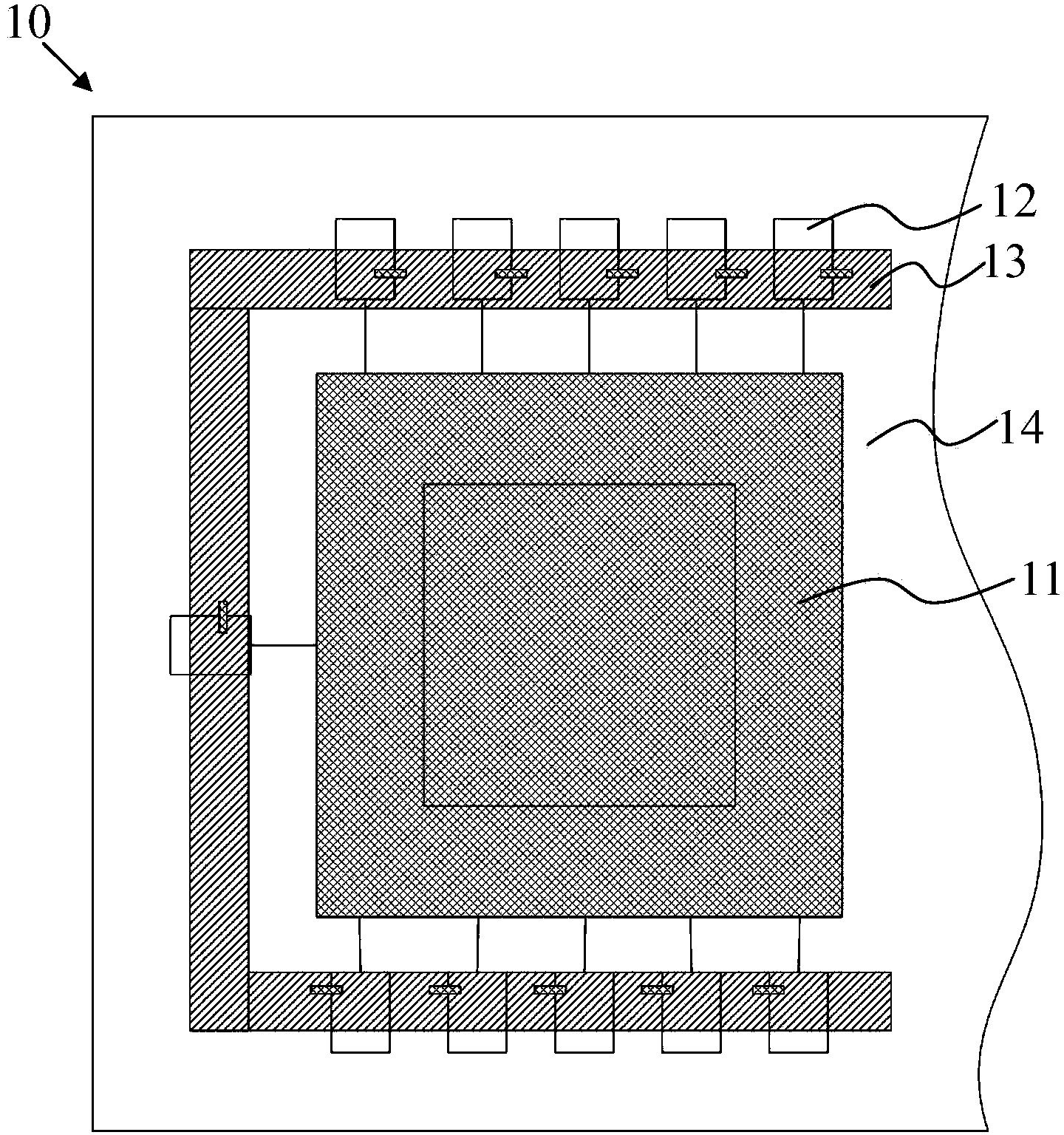
[0028] The following descriptions of the various embodiments refer to the accompanying drawings to illustrate specific embodiments in which the present invention can be practiced. The directional terms mentioned in the present invention, such as "up", "down", "front", "back", "left", "right", "inside", "outside", "side", etc., are for reference only The orientation of the attached schema. Therefore, the directional terms used are used to illustrate and understand the present invention, but not to limit the present invention.

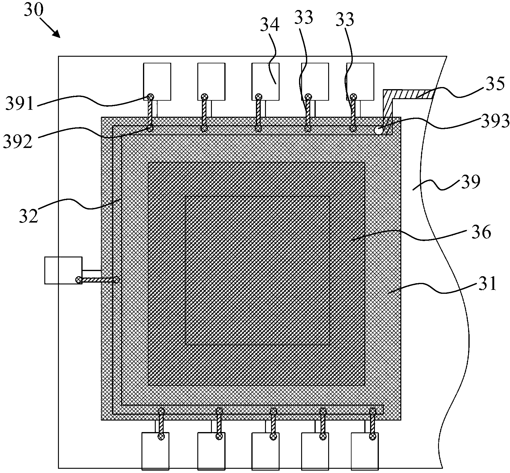
[0029] In the figures, structurally similar units are denoted by the same reference numerals.

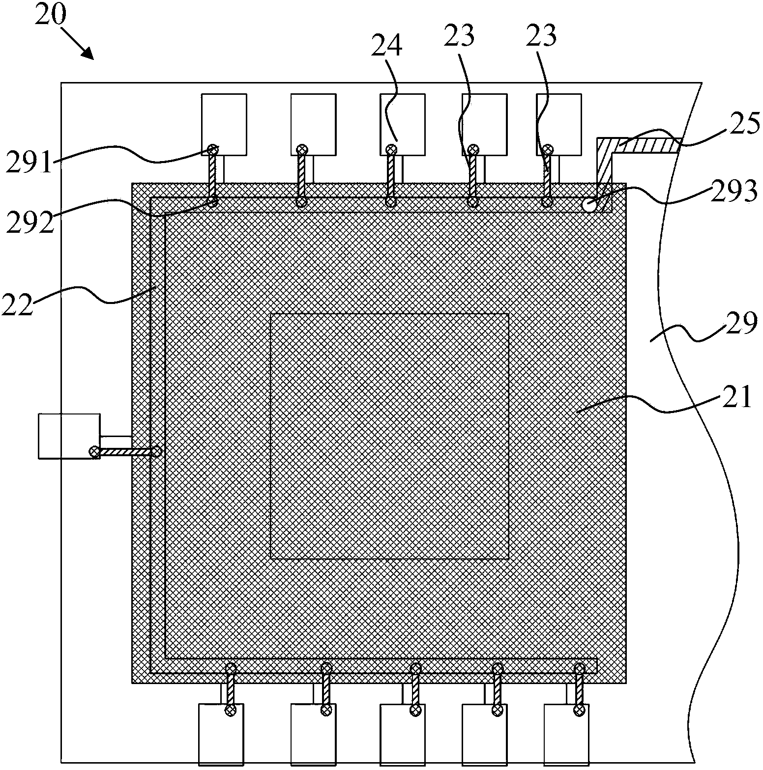
[0030] Please refer to figure 2 , figure 2 It is a structural schematic diagram of the first preferred embodiment of the chip structure of the present invention. The chip structure 20 is arranged on the corresponding printed circuit board 29, and the printed circuit board 29 includes a component layer and a copper foil ground layer, and the surface eleme...


PUM


Abstract

The invention provides a chip structure and a circuit structure. The chip structure is arranged on a printed circuit board provided with a part layer and a copper foil ground layer, and comprises a chip main body, a power supply line, power supply input lines and bypass capacitors, wherein the chip main body is arranged on the part layer and comprises a plurality of power supply pins; the power supply line is arranged on the part layer and used for supplying power to the chip main body; main bodies of the power supply input lines are arranged on the copper foil ground layer; two ends of the power supply input lines are arranged on the part layer; the main bodies of the power supply input lines are connected with the two ends of the power supply input lines by through holes in the printed circuit board; one end of each bypass capacitor is connected with the power supply pins of the chip main body by the part layer; and the other end of each bypass capacitor is connected with the power supply line by the power supply input lines. The invention further provides the circuit structure. The power supply line of the chip structure and a power supply line of the circuit structure are arranged on the part layer, so that a heat-dissipation effect of the copper foil ground layer is good, and production yields of a corresponding chip and a corresponding circuit are high.

Description

technical field [0001] The invention relates to the field of chip design, in particular to a chip structure and a circuit structure. Background technique [0002] With the increasingly fierce competition of chip products on the market, in order to reduce costs, the printed circuit boards of many chip products have been compressed into 2-layer boards, one layer is the component layer, and the other layer is the copper foil ground layer. Such as figure 1 as shown, figure 1 It is a structural schematic diagram of an existing chip structure. Single slashes are used in the figure to denote components on the copper ground plane. The chip structure 10 includes a chip 11 (indicated by double slashes) arranged on the component layer of the printed circuit board 14, a bypass capacitor 12 arranged near the power supply pin of the chip 11, and a power supply line arranged on the copper foil ground layer. 13 (indicated by a single slash); one end of the bypass capacitor 12 is connect...

Claims


Application Information

Patent Timeline
Patent Type & Authority Applications(China)
IPC IPC(8): H01L23/367H01L23/48H01L23/498
CPCH01L2924/37001H01L23/50H01L23/552H01L2924/19041H01L2924/19105H01L2924/0002H05K1/0209H05K1/0231H05K2201/09227H05K2201/10522H05K2201/10674H05K2201/10969H01L23/36H01L23/49838H05K2201/10015H01L2924/00H01L23/48H05K1/0203H05K1/092H05K1/115H05K1/18
Inventor 符俭泳
Owner TCL CHINA STAR OPTOELECTRONICS TECH CO LTD
Why Eureka
Try Eureka