CMOS (complementary metal-oxide semiconductor) image sensor

An image sensor and pixel technology, which is applied in the field of image sensors, can solve the problems of high equipment requirements, high cost, and high difficulty of through-silicon via technology, and achieve the effect of image quality optimization and a wide range of applications

Active Publication Date: 2014-01-22
SHANGHAI INTEGRATED CIRCUIT RES & DEV CENT
View PDF3 Cites 45 Cited by
  • Summary
  • Abstract
  • Description
  • Claims
  • Application Information

AI Technical Summary

Problems solved by technology

However, TSV technology is more difficult, has higher requirements for equipment, and its cost is relatively high

Method used


Image

  • CMOS (complementary metal-oxide semiconductor) image sensor
  • CMOS (complementary metal-oxide semiconductor) image sensor
  • CMOS (complementary metal-oxide semiconductor) image sensor

Examples


Embodiment Construction

[0028] In order to make the content of the present invention clearer and easier to understand, the content of the present invention will be further described below in conjunction with the accompanying drawings. Of course, the present invention is not limited to this specific embodiment, and general replacements known to those skilled in the art are also covered within the protection scope of the present invention.

[0029] figure 2 and image 3 is a schematic diagram of the pixel structure of the CMOS image sensor of the present invention.

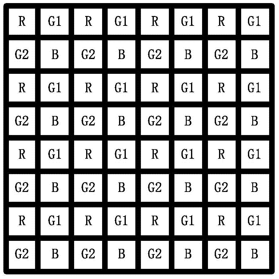
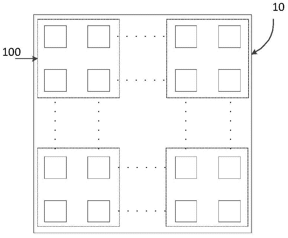
[0030] Such as figure 2 As shown, the CMOS image sensor 1 includes a pixel array 10 having a plurality of pixel units 100, and each pixel unit 100 includes a plurality of pixels.

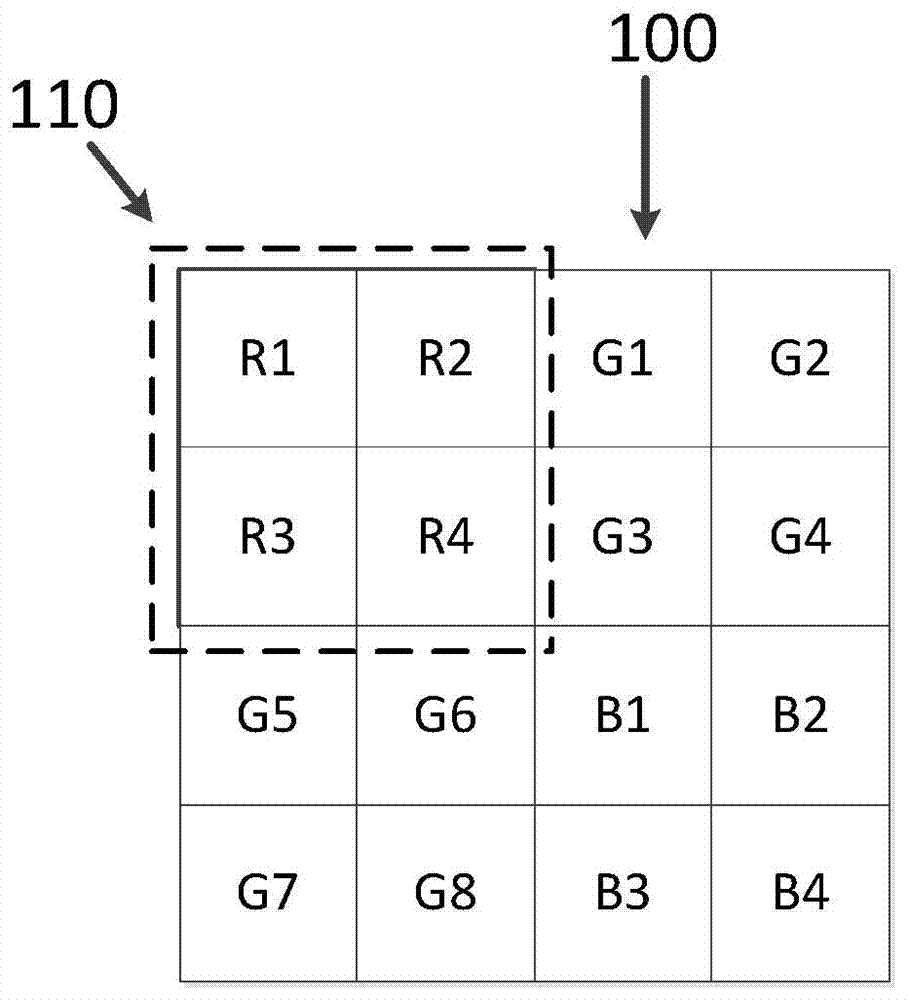
[0031] Please refer to image 3 , in this embodiment, each pixel unit 100 includes 4 pixels 110, and these 4 pixels are arranged in a Bayer distribution. Each pixel 110 is composed of 4 sub-pixels, and these 4 sub-pixels form a square. Specifically, the ...


PUM


Abstract

The invention discloses an image sensor which comprises a plurality of pixel units, control units and readout circuits, wherein each pixel unit comprises a plurality of pixels; each pixel comprises a plurality of sub-pixels; the readout circuits are correspondingly connected with the pixels and used for reading out a combined output signal of the sub-pixels of the pixels according to control signals sent from the control units or reading out the output signals of the sub-pixels of the pixels in sequence respectively. The image sensor has the advantages of capability of being switched between split and combined modes for meeting different requirements, and wider application range.

Description

technical field [0001] The invention relates to the field of image sensors, in particular to a CMOS image sensor. Background technique [0002] Image sensors are an important part of digital cameras. According to the different components, it can be divided into two categories: CCD (Charge Coupled Device, charge-coupled device) and CMOS (Complementary Metal-Oxide Semiconductor, metal oxide semiconductor device). A prerequisite for the wide application of CMOS sensors is their higher sensitivity, shorter exposure time and shrinking pixel size. [0003] Among them, the pixel sensitivity, one of the important performance indicators of the CMOS image sensor, is mainly determined by the product of the fill factor (the ratio of the photosensitive area to the entire pixel area) and the quantum efficiency (the number of electrons generated by the photons bombarding the screen). In CMOS image sensors, in order to achieve noise index and sensitivity level comparable to CCD converters...

Claims


Application Information

Patent Timeline
Patent Type & Authority Applications(China)
IPC IPC(8): H01L27/146
Inventor 李琛温建新赵宇航
Owner SHANGHAI INTEGRATED CIRCUIT RES & DEV CENT
Why Eureka
Try Eureka