Touch panel and touch display panel

A touch panel and display module technology, which is applied in the direction of instruments, electrical digital data processing, and input/output process of data processing, etc. It can solve problems such as the reduction of manufacturing engineering yield and the damage of touch panel components.

Inactive Publication Date: 2014-02-12
AU OPTRONICS CORP
View PDF3 Cites 14 Cited by
  • Summary
  • Abstract
  • Description
  • Claims
  • Application Information

AI Technical Summary

Problems solved by technology

[0003] Generally speaking, during the manufacturing process of the touch panel, when the electrostatic discharge phenomenon occurs, the components in the touch panel may be damaged, resulting in a decrease in the yield of the manufacturing process

Method used


Image

  • Touch panel and touch display panel
  • Touch panel and touch display panel
  • Touch panel and touch display panel

Examples


no. 1 approach

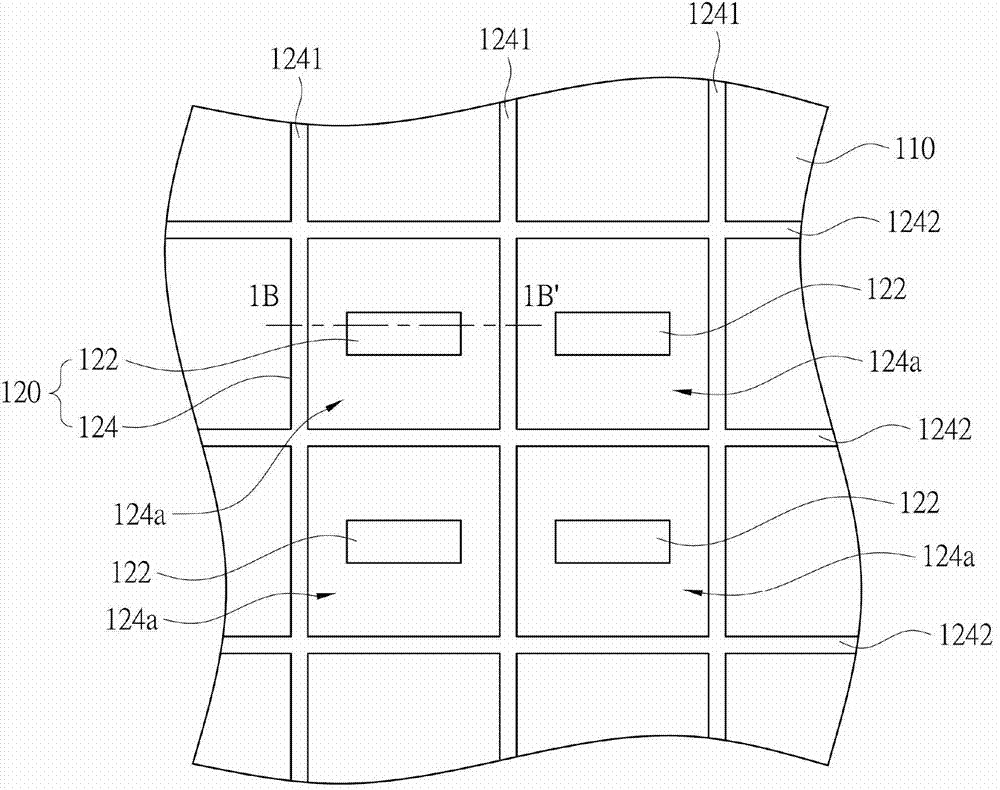
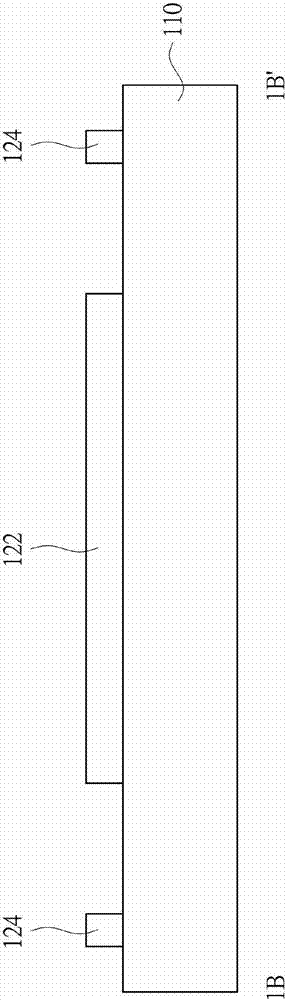
[0069] A first embodiment of the present invention provides a touch panel, which includes a substrate, a first conductive layer, an insulating layer, and a second conductive layer.

[0070] Figure 1A It is a schematic top view showing the first conductive layer 120 of this embodiment. Figure 1B to show along Figure 1A The schematic cross-sectional view of the line segment 1B-1B'. The first conductive layer 120 is disposed on the substrate 110 . The substrate 110 may be a glass substrate, a quartz substrate or a plastic substrate. The first conductive layer 120 can be made of transparent conductive material or metal. The transparent conductive material is, for example, indium tin oxide (ITO), indium zinc oxide (IZO), zinc oxide (ZnOx), indium gallium zinc oxide (IGZO), gallium zinc oxide (GZO), or a combination thereof. Metals such as molybdenum (Mo), chromium (Cr), neodymium (Nd), titanium (Ti), copper (Cu), silver (Ag), gold (Au), zinc (Zn), indium (In), gallium ( Ga),...

no. 2 approach

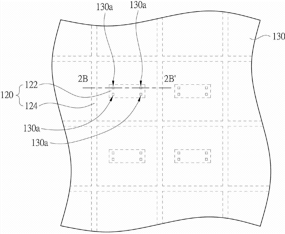
[0088] A second embodiment of the present invention provides a touch panel, which includes a substrate, a first conductive layer, an insulating layer, and a second conductive layer.

[0089] Figure 9A It is a schematic top view showing the first conductive layer 220 of this embodiment. Figure 9B to show along Figure 9A The schematic cross-sectional view of the line segment 9B-9B'. The first conductive layer 220 is disposed on the substrate 210 . The first conductive layer 220 includes a first sensing series 222 and at least two sensing pads 224 . The first sensing series 222 includes at least one bridge line 2222 and a plurality of sensing pads 2224 . The bridge wire 2222 connects two adjacent sensing pads 2224 in series to form a first sensing series 222 . The two sensing pads 224 are respectively located on opposite sides of the first sensing series 222 . Overall, the first conductive layer 220 may include a plurality of first sensing series 222 and a plurality of s...


PUM


Abstract

The invention provides touch panel comprises a substrate, a first conductive layer, a second conductive layer, and an insulation layer. The first conductive layer is disposed on the substrate, and the first conductive layer comprises a bridging line and a patterning static protective layer, which are separated from each other. The patterning static protective layer is provided with a floating potential or a grounding potential. The second conductive layer is disposed on the first conductive layer, and comprises a first sensing string and at least two sensing pads disposed on two opposite sides of the first sensing string. The insulation layer is disposed between the first conductive layer and the second conductive layer in a clamped manner. The insulation layer is provided with two contact holes. The bridging line is respectively connected with the adjacent two sensing pads to form a second sensing string. The invention also provides a touch control panel comprising the above mentioned touch panel and the display module.

Description

technical field [0001] The invention relates to a touch panel and a touch display panel. Background technique [0002] In recent years, touch technology has been widely used in various multimedia electronic products, especially portable mobile products, such as mobile phones, e-books, and tablet computers. Using touch technology as an input means can effectively replace the existing keyboard or mouse input means. In addition to convenience, touch input technology has become a very popular way of man-machine interface and multimedia interaction due to its intuitive operation. [0003] Generally speaking, during the manufacturing process of the touch panel, when the electrostatic discharge phenomenon occurs, the components in the touch panel may be damaged, resulting in a decrease in the yield of the manufacturing process. Since the phenomenon of electrostatic discharge cannot be completely avoided in the manufacturing process and in the process of use, how to make a touch p...

Claims


Application Information

Patent Timeline
Patent Type & Authority Applications(China)
IPC IPC(8): G06F3/041
Inventor 陈建宇庄文奇林怡伶
Owner AU OPTRONICS CORP
Why Eureka
Try Eureka