Supercharge Your Innovation With Domain-Expert AI Agents!

Laminated ceramic electronic component and method of fabricating the same

A technology of ceramic electronic components and ceramic powder, which is applied in the direction of electrical components, multilayer capacitors, fixed capacitor parts, etc. Decreased withstand voltage characteristics, etc.

Active Publication Date: 2014-02-12
SAMSUNG ELECTRO MECHANICS CO LTD
View PDF10 Cites 3 Cited by
  • Summary
  • Abstract
  • Description
  • Claims
  • Application Information

AI Technical Summary

Problems solved by technology

[0007] In this case, the surface roughness of the dielectric layer can be gradually reduced, but the adhesion between the dielectric layer and the internal electrodes will also decrease accordingly
[0008] In this way, in the manufacturing process of laminated ceramic electronic components, it will cause delamination of dielectric layers and internal electrodes, which will reduce the reliability of laminated ceramic electronic components
[0009] Also, using only fine ceramic powder particles may lower the dielectric constant
[0010] On the other hand, when the ceramic powder used has relatively large particles, as the surface roughness of the dielectric layer increases, the withstand voltage characteristics may be reduced

Method used


Image

  • Laminated ceramic electronic component and method of fabricating the same
  • Laminated ceramic electronic component and method of fabricating the same
  • Laminated ceramic electronic component and method of fabricating the same

Examples


Embodiment Construction

[0037] Embodiments of the present invention will be described in detail below with reference to the accompanying drawings. This invention may, however, be embodied in many different forms and should not be construed as limited to the embodiments set forth herein. Rather, these embodiments are provided so that this disclosure will be thorough and complete, and will fully convey the scope of the invention to those skilled in the art.

[0038] In the drawings, the shapes and dimensions of elements may be exaggerated for clarity, and the same reference numerals will be used throughout to identify the same or like elements.

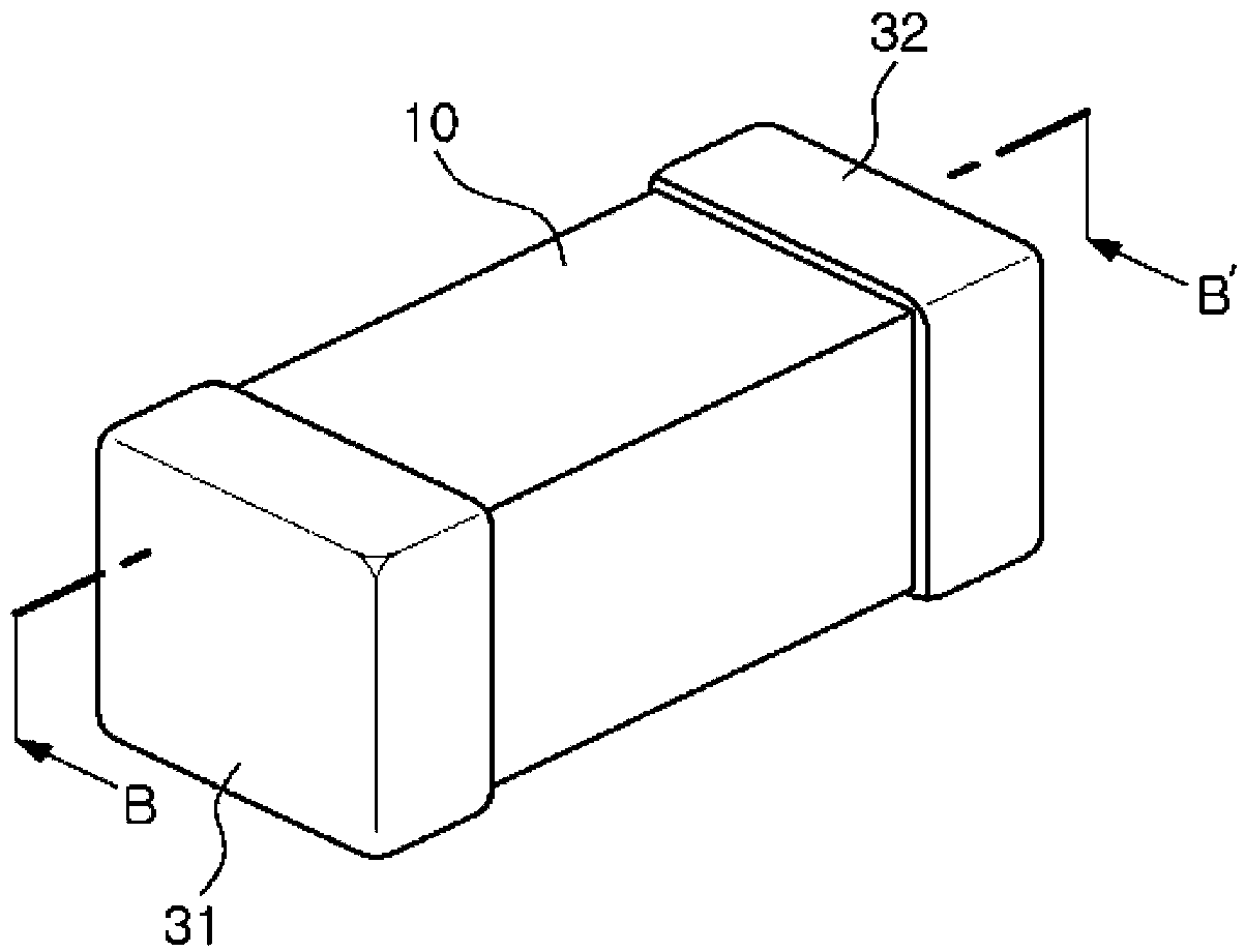
[0039] figure 1 is a perspective view schematically showing a laminated ceramic capacitor according to an embodiment of the present invention;

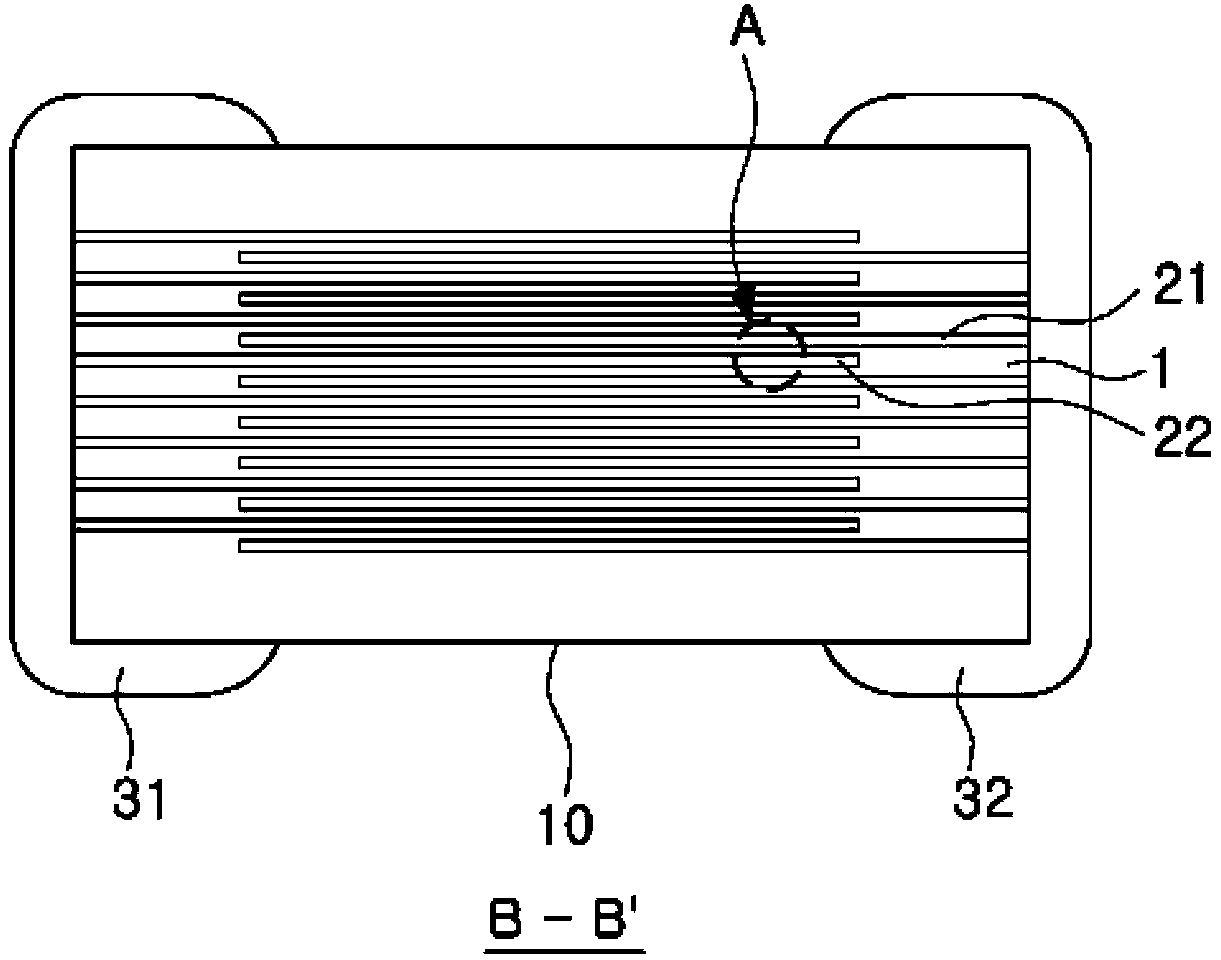
[0040] figure 2 is along figure 1 Sectional view taken along line B-B' in ;

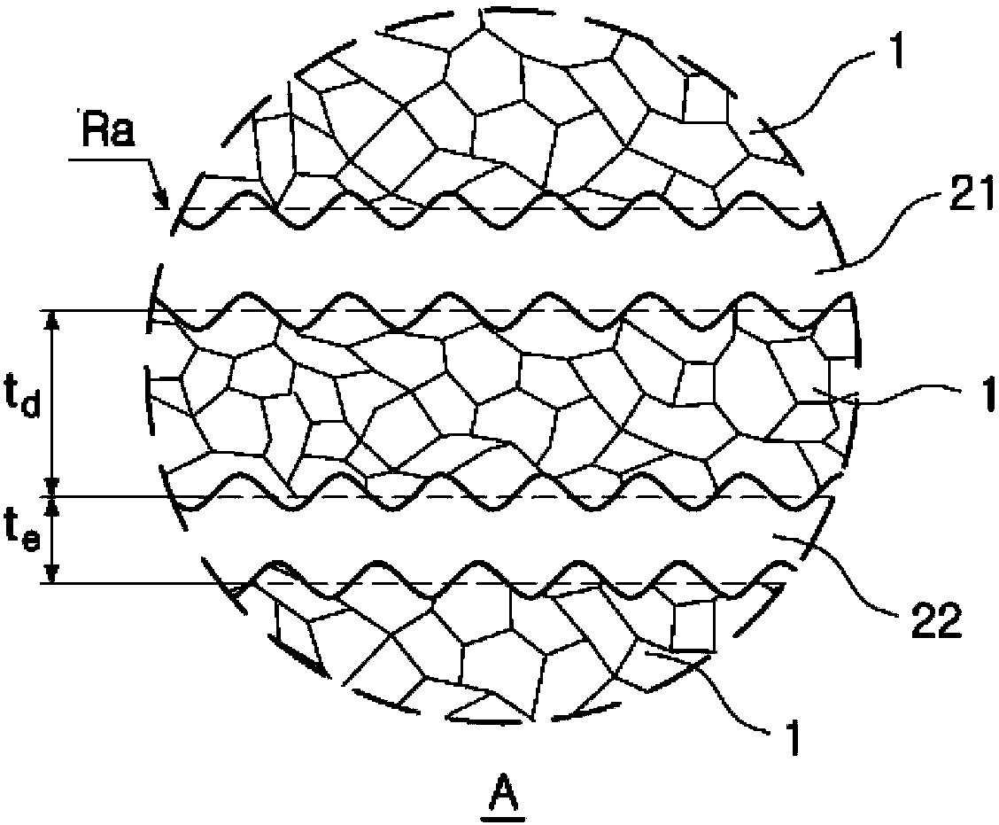
[0041] image 3 is displayed figure 2 A magnified view of the thickness of the internal electrode layer and dielectric layer in . ...


PUM

PropertyMeasurementUnit
roughnessaaaaaaaaaa
roughnessaaaaaaaaaa
particle diameteraaaaaaaaaa

Abstract

There is provided a laminated ceramic electronic component, including a ceramic body including a dielectric layer; and first and second internal electrodes disposed to face each other, having the dielectric layer interposed therebetween within the ceramic body, wherein when a value of 1% is set to be D1, a value of 50% is set to be D50, and a value of 99% is set to be D99 in a cumulative distribution of dielectric grains by an average particle diameter thereof within the dielectric layer, 2@D99 / D50@3 and 2@D50 / D1@3 are satisfied. A high-capacity laminated ceramic electronic component may be implemented with improved adhesion between the dielectric layer and the internal electrode, and improved withstand voltage characteristics and excellent reliability may be implemented.

Description

[0001] Cross References to Related Applications [0002] This application claims priority to Korean Patent Application No. 10-2012-0079527 filed Jul. 20, 2012 at the Korean Intellectual Property Office, the entire contents of which are hereby incorporated by reference herein Application. technical field [0003] The present invention relates to a high-capacitance laminated ceramic electronic component having improved withstand voltage characteristics and excellent reliability. Background technique [0004] Recently, as electronic products have been miniaturized, demands for small, high-capacitance laminated ceramic electronic components have increased. [0005] Therefore, thinning and lamination of dielectrics and internal electrodes have been attempted by various methods. Currently, laminated ceramic electronic components having thinned dielectric layers and laminates with an increased number of layers have been manufactured. [0006] In addition, in order to achieve thi...

Claims


Application Information

Patent Timeline
Patent Type & Authority Applications(China)
IPC IPC(8): H01G4/005H01G4/12H01G4/30
CPCH01G4/12H01G4/30C04B35/468H01G4/1227C04B2235/5445C04B2235/5454C04B2235/5472C04B2235/782C04B2235/784C04B2235/785Y10T156/1092
Inventor 郑汉胜金昶勋权祥勋尹硕晛
Owner SAMSUNG ELECTRO MECHANICS CO LTD
Features
  • R&D
  • Intellectual Property
  • Life Sciences
  • Materials
  • Tech Scout
  • Unparalleled Data Quality
  • Higher Quality Content
  • 60% Fewer Hallucinations
Learn More