

Photoluminescent device and production method thereof
A technology of photoluminescence and devices, which is applied in the field of luminescence, can solve problems such as low luminous efficiency, low luminous efficiency, and difficulty in meeting the needs of use, and achieve the effect of improving luminous efficiency
- Summary
- Abstract
- Description
- Claims
- Application Information
AI Technical Summary
Problems solved by technology
Method used
Image

Examples
preparation example Construction
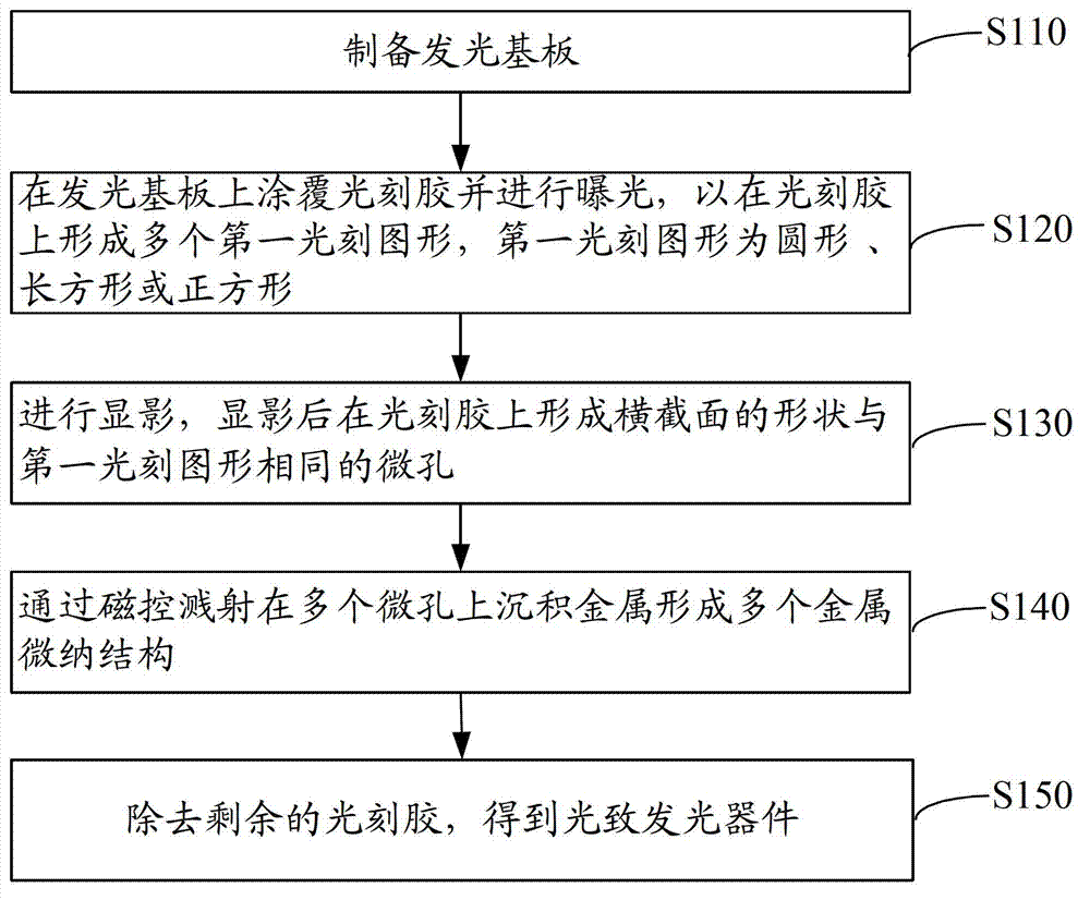
[0037] see figure 2 , the preparation method of the photoluminescence device of an embodiment, comprises the following steps:
[0038] Step S110: preparing a light-emitting substrate.
[0039] The luminescent substrate is composed of luminescent glass, luminescent transparent glass ceramics (glass ceramics), luminescent transparent ceramics, or transparent glass and a luminescent film laminated on the transparent glass.
[0040] When the luminescent substrate is luminescent glass, luminescent transparent glass ceramics (glass ceramics) or luminescent transparent ceramics, the luminescent substrate is made of luminescent materials by high temperature melting method or high temperature and high pressure method, such as red light material Y 2 o 3 :Eu 3+ , Y 2 o 2 S:Eu 3+ Red light emitting glass, red light emitting transparent glass ceramics (glass ceramics) or red light emitting transparent ceramics doped with glass, transparent glass ceramics or transparent ceramics.
...
Embodiment 1
[0063] Preparation of photoluminescent device 100
[0064] Please also see Figure 3~Figure 5 , preparing the photoluminescent device 100 includes the following steps:
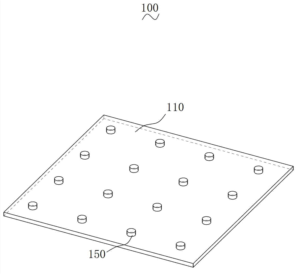
[0065] (1) The red luminescent material Y is made by high-temperature melting method 2 o 3 :Eu 3+ Doping in glass to prepare luminescent glass as a luminescent substrate 110, the length, width and height of the luminescent substrate 110 is 5cm×5cm×0.1cm, cleaning the luminescent substrate 110 and drying;
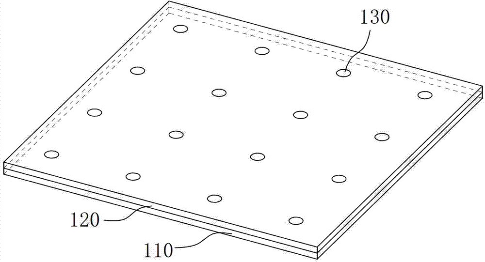
[0066] (2) coating a photoresist with a thickness of 50 nm on the light-emitting substrate 110 by spin coating to form a photoresist layer 120;
[0067] (3) 16 first photoresist patterns 130 arranged in a square (four rows and four columns, row spacing and column spacing are both 400nm) are exposed on the photoresist layer 120 by ultraviolet light, and the first photolithography patterns 130 are A circular shape with a diameter of 400 nm, such as image 3 shown;
[0068] (4) Soak and develop with KOH ...
Embodiment 2
[0072] A photoluminescent device is prepared, comprising the steps of:
[0073] (1) Provide a glass substrate. After cleaning the glass substrate and drying it, use screen printing to print the luminescent material on the glass substrate to form a luminescent film or use magnetron sputtering to make the luminescent material Y 2 o 3 :Eu 3+ Deposit on the surface of the glass substrate to form a luminescent film to obtain a luminescent substrate. The length, width and height of the light-emitting substrate are 5cm×5cm×0.1cm;
[0074] (2) Coating a photoresist with a thickness of 50 nm on the luminescent film by spin coating to form a photoresist layer;
[0075] (3) Expose 16 first photolithographic patterns arranged in a square (four rows and four columns, with a row spacing and a column spacing of 1μnm) on the photoresist layer by ultraviolet light. The first photolithographic pattern has a diameter of 400nm round shape;
[0076] (4) Soak and develop with KOH solution, and...
PUM
| Property | Measurement | Unit |
|---|---|---|
| Thickness | aaaaa | aaaaa |
| Bottom diameter | aaaaa | aaaaa |
Abstract
Description
Claims
Application Information