Nitride semiconductor device

A nitride semiconductor and electrode technology, which is applied in the direction of semiconductor devices, semiconductor/solid-state device manufacturing, semiconductor/solid-state device components, etc., can solve the problems of inability to miniaturize, limited reduction of electrode pads, and large area, etc., to achieve Effects of prevention of electromigration, suppression reduction, and on-resistance reduction

Active Publication Date: 2014-02-19
PANASONIC INTELLECTUAL PROPERTY MANAGEMENT CO LTD
View PDF3 Cites 0 Cited by
  • Summary
  • Abstract
  • Description
  • Claims
  • Application Information

AI Technical Summary

Problems solved by technology

However, conventional III-V nitride semiconductor devices have a problem that the area occupied by the electrode pads for connection wiring is large, and thus cannot be sufficiently miniaturized.
In particular, in the application as a power device through which a large current flows, since the diameter of the wire connected to the electrode pad and the size of the ribbon are preferably large, the extent to which the electrode pad can be reduced is limited.

Method used


Image

  • Nitride semiconductor device
  • Nitride semiconductor device
  • Nitride semiconductor device

Examples


no. 1 approach

[0047] refer to Figure 1 ~ Figure 3 The nitride semiconductor device according to the first embodiment of the present invention will be described.

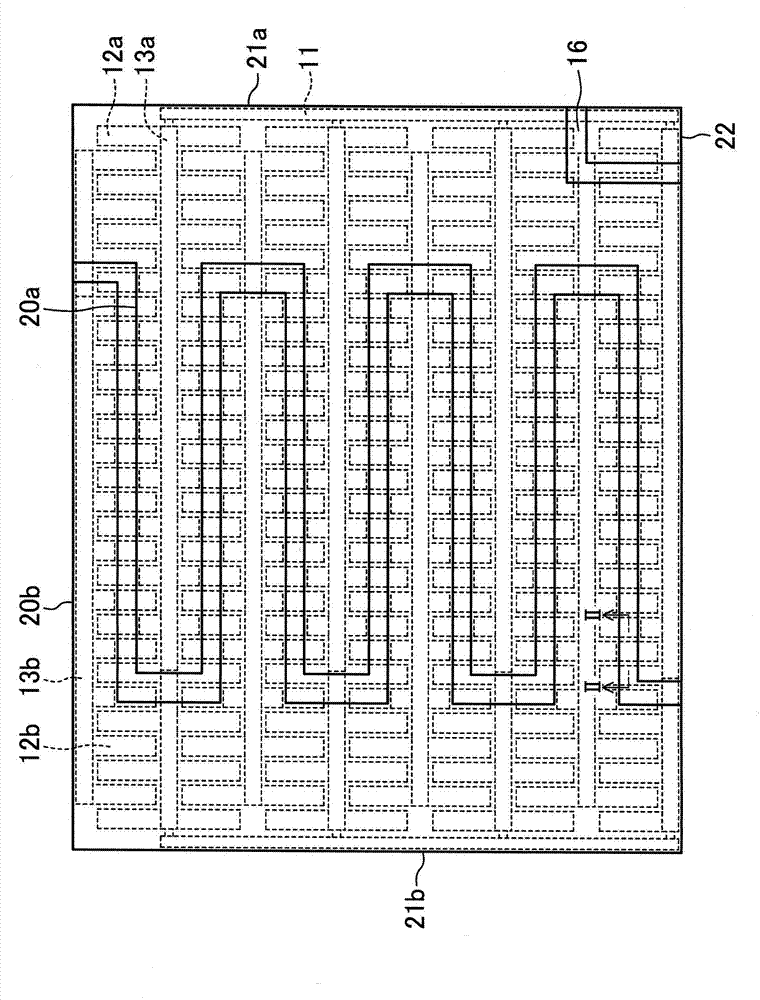
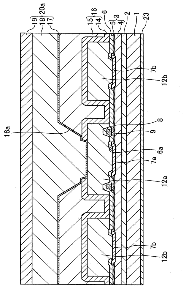
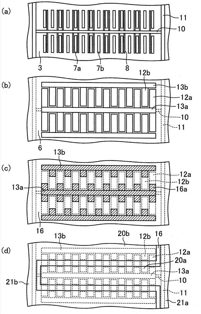
[0048] Such as figure 1 as well as figure 2 As shown, in the nitride semiconductor device of the first embodiment, a buffer layer 2 and a nitride semiconductor layer 3 are sequentially formed on a substrate 1 formed of, for example, silicon (Si). The nitride semiconductor layer 3 is composed of an undoped gallium nitride (GaN) layer 4 with a thickness of about 2.5 μm and an undoped aluminum gallium nitride (AlGaN) layer 5 with a thickness of about 50 nm formed thereon. A two-dimensional electron gas (2DEG) is generated in the interface region between the undoped GaN layer 4 and the undoped AlGaN layer 5 , and the 2DEG functions as a channel region.

[0049] On the nitride semiconductor layer 3 , source electrodes 7 a as first electrodes and drain electrodes 7 b as second electrodes are separated from each other and alternatel...

no. 2 approach

[0065] Below, refer to Figure 4 as well as Figure 5 A nitride semiconductor device according to a second embodiment of the present invention will be described. In the present embodiment, the same reference numerals are attached to the same components as in the first embodiment, and description thereof will be omitted, and only different parts will be described.

[0066] The nitride semiconductor device according to the second embodiment of the present invention is a double gate type nitride semiconductor device having two gate electrodes, the first gate electrode G1 electrode 38a and the second gate electrode G2 electrode 38b. Such as Figure 4 as well as Figure 5 As shown, a G1 electrode pad 52a and a G2 electrode pad 52b electrically connected to the G1 electrode 38a and the G2 electrode 38b are formed on the active region. Similarly, an S1 electrode pad 51a and an S2 electrode pad 51b electrically connected to the S1 electrode 37a as the first electrode and the S2 el...


PUM


Abstract

This nitride semiconductor device is provided with: first electrode wiring layers, which are formed parallel to each other on a nitride semiconductor layer, and are divided in the longitudinal direction, respectively; a first gate electrode formed along the first electrode wiring layers; first gate electrode collective wiring, which is formed in regions where the first electrode wiring layers are divided, and is connected to the first gate electrode; first electrode collective wiring (13a), which is formed on the first gate electrode collective wiring, and is connected to the first electrode wiring layers; and first electrode upper layer wiring (20a), which is formed on an insulating film (16) on the wiring, said insulating film being formed on the first electrode collective wiring, and is connected to the first electrode collective wiring through an opening in the insulating film on the wiring.

Description

technical field [0001] The present invention relates to a nitride semiconductor device, and more particularly, to a nitride semiconductor device having an electrode pad formed on an active region. Background technique [0002] With the general formula Al x Ga 1-x-y In y N (here, 0≤x≤1, 0≤y≤1, and 0≤x+y≤1) represents a III-V group nitride semiconductor, since it has a wide band gap and a direct transition as its physical characteristics The type of energy band structure, therefore, is applied in short-wavelength optical elements. Furthermore, since group III-V nitride semiconductors have characteristics of a high breaking electric field and a high saturation electron velocity, researches on application to electronic devices and the like are also underway. [0003] In particular, the use of aluminum gallium nitride (AlGaN) sequentially epitaxially grown on a semi-insulating substrate is being developed as a high-output device and a high-frequency device. x Ga 1-x N, here...

Claims


Application Information

Patent Timeline
Patent Type & Authority Applications(China)
IPC IPC(8): H01L21/338H01L21/3205H01L21/768H01L23/522H01L29/778H01L29/812
CPCH01L29/41758H01L29/7787H01L29/812H01L23/4824H01L2924/0002H01L2924/00H01L23/5226H01L23/528H01L29/42356
Inventor 海原一裕按田义治
Owner PANASONIC INTELLECTUAL PROPERTY MANAGEMENT CO LTD
Why Eureka
Try Eureka