Stacked encapsulation structure and manufacturing method thereof

一种层叠封装、制作方法的技术,应用在半导体/固态器件制造、半导体/固态器件零部件、半导体器件等方向,能够解决影响电连接性能、降低层叠封装结构成品率及可靠性等问题

Active Publication Date: 2014-03-12
LEADING INTERCONNECT SEMICON TECH SHENZHEN CO LTD +2
View PDF4 Cites 6 Cited by
  • Summary
  • Abstract
  • Description
  • Claims
  • Application Information

AI Technical Summary

Problems solved by technology

Due to the long length of the through hole, the conductive paste is not easy to fill the through hole, and it is easy to generate more air bubbles, thereby affecting the electrical connection performance between the upper package device and the lower package device, thereby reducing the yield of the stacked package structure and reliability

Method used


Image

  • Stacked encapsulation structure and manufacturing method thereof
  • Stacked encapsulation structure and manufacturing method thereof
  • Stacked encapsulation structure and manufacturing method thereof

Examples


Embodiment Construction

[0023] The package-on-package structure provided by the technical solution and its manufacturing method will be further described in detail below in conjunction with the accompanying drawings and embodiments.

[0024] The manufacturing method of the package-on-package structure provided by the first embodiment of the present invention includes the following steps:

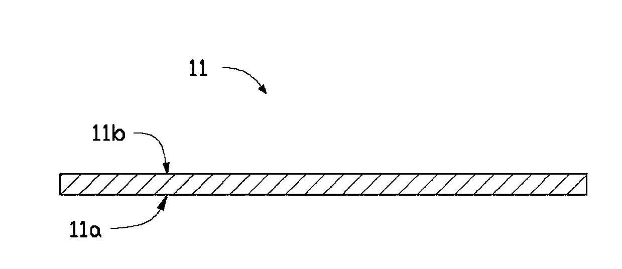
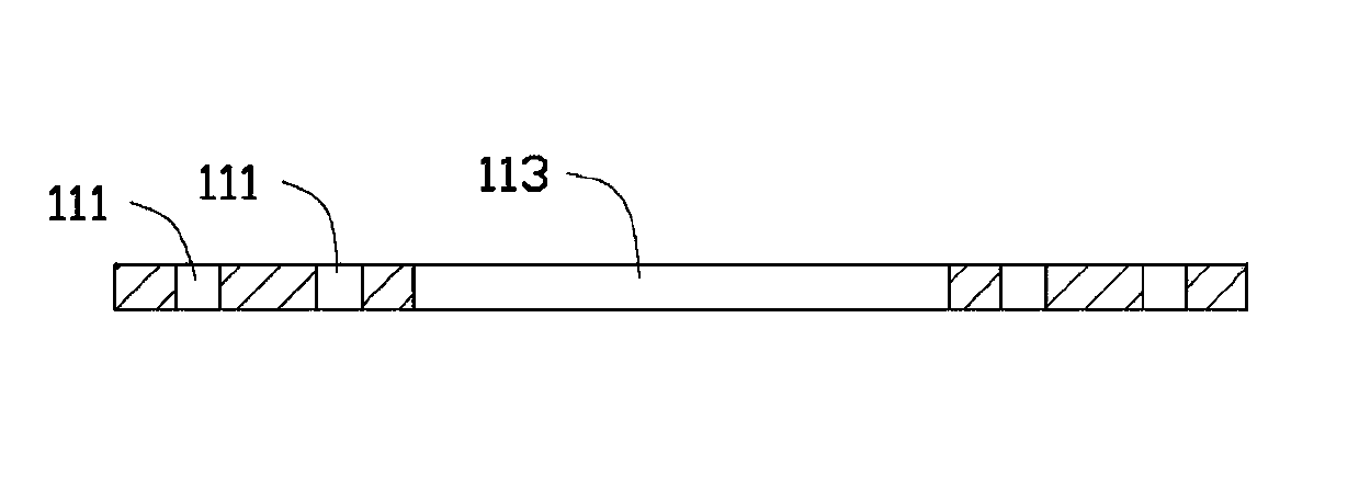
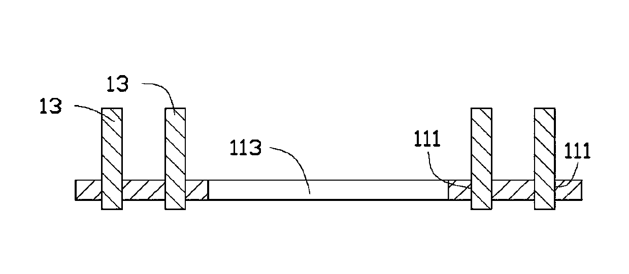
[0025] Step 1: Please also refer to Figure 1 to Figure 3, providing a connection substrate 10 . The connection substrate 10 includes a substrate body 11 and a plurality of conductive posts 13 disposed in the substrate body 11 . The substrate body 11 has a first surface 11a and a second surface 11b opposite to each other. The substrate body 11 defines a plurality of first receiving through holes 111 and a second receiving through hole 113 . Each of the plurality of first receiving through holes 111 and one second receiving through hole 113 runs through the first surface 11a and the second surface 11b, and the pl...


PUM


Abstract

The invention provides a manufacturing method of a stacked encapsulation structure. The manufacturing method comprises the following steps that: a connection substrate is provide, wherein the connection substrate includes a substrate body and a plurality of conductive columns arranged in the substrate body; one side of a first surface of the connection substrate is provided a first encapsulation device; one side of a second surface of the connection substrate is provided with an encapsulation colloid, such that a semi-finished stacked encapsulation structure can be formed; and one side of the encapsulation colloid, which is far away from the encapsulation device, is provided with a second encapsulation device, such that the stacked encapsulation structure can be formed. The invention also relates to a stacked encapsulation structure formed through using the above method.

Description

technical field [0001] The invention relates to a semiconductor packaging technology, in particular to a package-on-package (POP) structure and a manufacturing method thereof. Background technique [0002] With the continuous reduction of the size of semiconductor devices, the package-on-package structure with semiconductor devices is gradually attracting attention. Package-on-package structures are generally fabricated by a stack-up fabrication method. In the traditional stacking method, in order to achieve high-density integration and small-area installation, the upper package device and the lower package device are usually mechanically connected through the epoxy molding compound layer, and the upper package device is connected through the conductive pillars in the epoxy molding compound layer. and the lower packaging device are electrically connected. The epoxy molding compound layer has a plurality of through holes for accommodating the conductive pillars. The conduc...

Claims


Application Information

Patent Timeline
Patent Type & Authority Applications(China)
IPC IPC(8): H01L21/60H01L21/56H01L23/31H01L23/538
CPCH01L2924/15311H01L25/105H01L21/4853H01L2224/73204H01L2225/1023H01L2224/32225H01L23/49811H01L2225/1058H01L2224/16225H01L23/49822H01L23/49833H01L23/3128H01L23/49827H01L24/11H01L21/76885H01L23/5386H01L2924/181H01L2924/12042H01L2224/16235H01L2224/16237H01L2924/00012H01L2924/00H01L24/29H01L2225/107
Inventor 陈建志石红霞许诗滨
Owner LEADING INTERCONNECT SEMICON TECH SHENZHEN CO LTD
Why Eureka
Try Eureka