Circuit for compensating nonlinear capacitance to reduce harmonic distortion to greatest extent

A technology of nonlinear capacitance and harmonic distortion, which is applied in improving amplifiers to reduce nonlinear distortion, logic circuit connection/interface layout, etc., and can solve the problems of circuit limitation, high cost, and multi-space.

Inactive Publication Date: 2014-03-12
SUZHOU BATELAB MICROELECTRONICS
View PDF2 Cites 4 Cited by
  • Summary
  • Abstract
  • Description
  • Claims
  • Application Information

AI Technical Summary

Problems solved by technology

One disadvantage of this simple MOS transistor T / H circuit is that the parasitic capacitance of the transistor varies non-linearly with the voltage across the transistor junction
However, not only does this approach require more space and cost more, but there are also limitations to the circuits to which it can be applied

Method used


Image

  • Circuit for compensating nonlinear capacitance to reduce harmonic distortion to greatest extent
  • Circuit for compensating nonlinear capacitance to reduce harmonic distortion to greatest extent
  • Circuit for compensating nonlinear capacitance to reduce harmonic distortion to greatest extent

Examples


Embodiment Construction

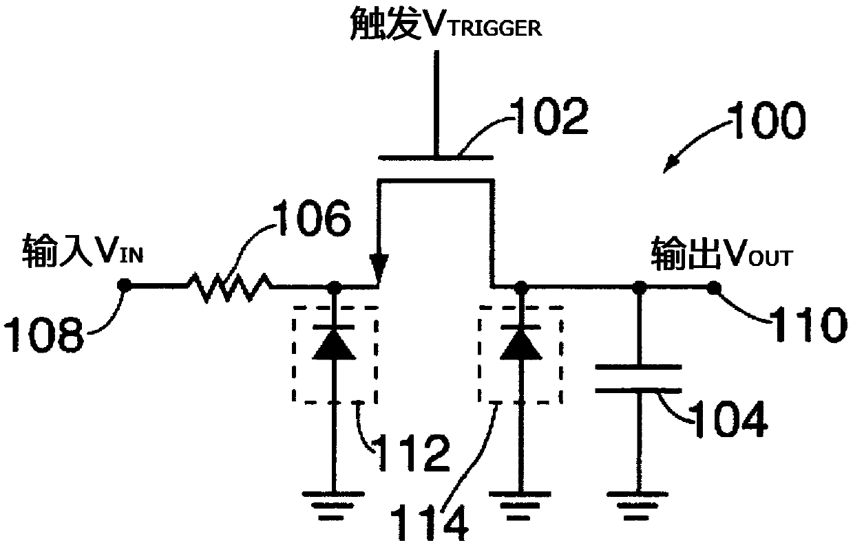
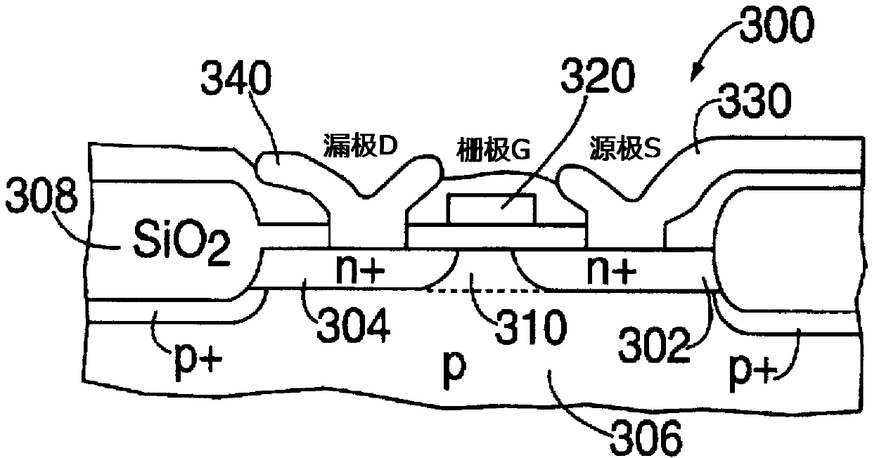
[0023] figure 1 is a simplified schematic of a typical track and hold circuit. Such as figure 1 As shown, the T / H circuit 100 employs a metal oxide semiconductor (MOS) transistor 102 and a capacitor 104 . Resistor 106 represents the input source impedance. MOS transistor 102 also includes parasitic junction capacitances at the drain and source, represented by PJC diodes 112 and 114, respectively. In the figure, PJC diodes 112 and 114 are shown by dashed boxes, which represent the pn junction of MOS transistor 102 .

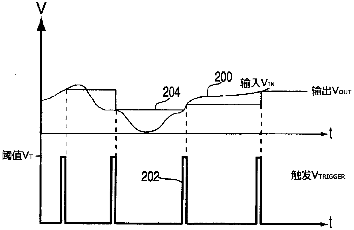
[0024] Ideally, an input signal V IN resulting in a voltage change at the input node 108 . When the gate of MOS transistor 102 is coupled to a voltage greater than the voltage at input node 108, MOS transistor 102 acts like a resistor—allowing capacitor 104 to charge and discharge such that the output V at output node 110 OUT With the input signal V IN change (i.e. tracking mode). When the gate of the MOS transistor 102 is coupled to a voltage less than th...


PUM


Abstract

Provided is a circuit for compensating nonlinear capacitance to reduce harmonic distortion to the greatest extent. The circuit can improve stray capacitance between transistors and is independent of the adopted process technology. In a preferential instance, a pair of diodes with inversely proportional actions is provided for a parasitic diode in an integrated circuit during operation, so stray capacitance of the transistors in the circuit is linearized. If the diodes do not exist in the circuit, different input signals can give rise to changes of the stray capacitance, and therefore harmonic distortion of the circuit is caused. Another embodiment of the invention further provides a complementary transistor. The complementary transistor forms another stray capacitance which is basically opposite to the stray capacitance in the transistors. In addition, according to proportions of different elements, the two methods can be combined, for instance, the diodes can be added while the complementary transistor is used.

Description

Technical field: [0001] This invention relates to the parasitic capacitance of transistors, particularly in track and hold (T / H) circuits or other circuits in combination with T / H circuits. More specifically, the present invention relates to circuits and methods for minimizing non-linear capacitance in T / H and other circuits. Background technique: [0002] T / H circuits are used to maintain a constant amplitude output based on the input, such as in an analog-to-digital converter (ADC). Therefore, the T / H circuit may have high system accuracy requirements, including the accuracy of any data created by the ADC. The T / H circuit generally operates in two different modes, namely "tracking mode" and "holding mode". In tracking mode, the T / H circuit generally acts as an input voltage follower. In hold mode, the T / H circuit holds this input signal as an output signal when time hold mode is activated. T / H circuits typically switch between modes with simple flip-flops. When the T / ...

Claims


Application Information

Patent Timeline
Patent Type & Authority Applications(China)
IPC IPC(8): H03F1/32H03K19/0175
Inventor 不公告发明人
Owner SUZHOU BATELAB MICROELECTRONICS
Why Eureka
Try Eureka