A kind of i/o interface circuit of asynchronous sram

An interface circuit and asynchronous technology, applied in the direction of information storage, static memory, digital memory information, etc., can solve the problems of high power consumption, poor reliability, and unstable control of I/O interface circuits, so as to reduce power consumption and enhance accuracy performance, speed up the response

Active Publication Date: 2016-08-24
BEIJING ZHONGKE XINWEITE SCI & TECH DEV
View PDF4 Cites 0 Cited by
  • Summary
  • Abstract
  • Description
  • Claims
  • Application Information

AI Technical Summary

Problems solved by technology

[0003] In order to solve the problems of large power consumption, poor reliability and unstable control of the existing I / O interface circuit of the asynchronous SRAM, the present invention provides an I / O interface circuit of the asynchronous SRAM, including a read circuit and a write circuit; The output end of the read circuit is connected to the input end of the write circuit; the read circuit is connected to the enable signal, the data signal and the read signal; the write circuit is connected to the write signal

Method used


Image

  • A kind of i/o interface circuit of asynchronous sram
  • A kind of i/o interface circuit of asynchronous sram
  • A kind of i/o interface circuit of asynchronous sram

Examples


Embodiment Construction

[0012] The technical solutions of the present invention will be further described below in conjunction with the accompanying drawings and embodiments.

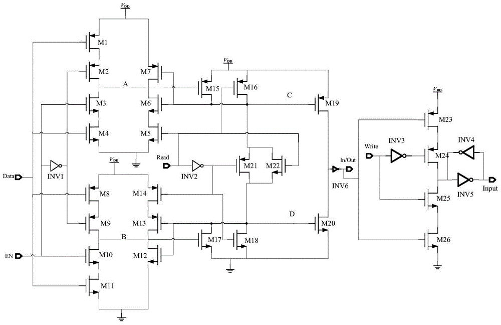
[0013] An embodiment of the present invention provides an I / O interface circuit of an asynchronous SRAM, including a read circuit and a write circuit. Wherein, the output terminal of the reading circuit is connected with the input terminal of the writing circuit; the reading circuit is connected with the enable signal EN, the data signal Data and the reading signal Read; the writing circuit is connected with the writing signal Write.

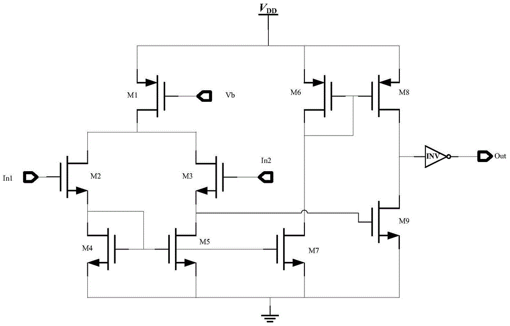
[0014] see figure 2, the read circuit includes a first PMOS transistor M1, a second PMOS transistor M2, a third NMOS transistor M3, a fourth NMOS transistor M4, a fifth NMOS transistor M5, a sixth NMOS transistor M6, a seventh PMOS transistor M7, an eighth PMOS transistor Transistor M8, ninth PMOS transistor M9, tenth NMOS transistor M10, eleventh NMOS transistor M11, twelfth NMOS transistor M...


PUM


Abstract

The invention discloses an I / O interface circuit of an asynchronous SRAM, belonging to the technical field of SRAM data reading and writing. The interface circuit includes a read circuit and a write circuit; the output end of the read circuit is connected to the input end of the write circuit; the read circuit is connected to the enable signal, the data signal and the read signal; the write circuit is connected to the write signal . The I / O interface circuit of the asynchronous SRAM of the present invention controls the operation of the output data by using the enable signal and the read signal, and uses the write signal to control the write operation of the data, so that the read or write of the data is realized conveniently and quickly Operation; by introducing positive feedback in the read circuit, the accuracy of the level signal is enhanced; there is no path from the power supply VDD to the ground GND, which greatly reduces the power consumption of the read circuit; by using the read signal to control the transistor Turn on to speed up the response speed of the circuit.

Description

technical field [0001] The invention relates to the technical field of SRAM data reading and writing, in particular to an I / O interface circuit of an asynchronous SRAM. Background technique [0002] The I / O interface circuit of SRAM (Static Random Access Memory, SRAM) is bidirectional, and the data stored in SRAM can be used as input or output. In engineering applications, the driving problem of the signal should also be considered. figure 1 It is the I / O interface circuit diagram of the existing asynchronous SRAM, in the I / O interface circuit by designing the gate voltage V of the PMOS tube M1 b Make it work in a saturated state, which is equivalent to a constant current source, and M2~M5 constitute a differential signal amplifier; the differential amplified signal of In1 and In2 is output to the gate of M9, if it is high level, the drain terminal of M9 Pull down to the ground, and then output the correct signal to Out through the inverter INV; and the two groups of M6 an...

Claims


Application Information

Patent Timeline
Patent Type & Authority Patents(China)
IPC IPC(8): G11C11/4063G11C7/10G11C7/22
Inventor 刘鑫赵发展刘梦新韩郑生
Owner BEIJING ZHONGKE XINWEITE SCI & TECH DEV
Why Eureka
Try Eureka