Method for solving short circuit of signal through hole and packaging bonding pad

A signal via hole and soldering technology, which is applied to printed circuit components, electrical connection printed components, etc., can solve problems such as PCB board burnout, open flame burning, function debugging, etc., to ensure quality, avoid short circuits, and improve reliability Effect

Inactive Publication Date: 2014-03-19
GUANGDONG VTRON TECH CO LTD
View PDF5 Cites 4 Cited by
  • Summary
  • Abstract
  • Description
  • Claims
  • Application Information

AI Technical Summary

Problems solved by technology

In the actual actual use process, it often happens that the PCB board directly hits the large pad of the LDO because of the via hole, which causes the device to burn out and the PCB board burns out after power on. When a short circuit burns out, It is impossible to carry out subsequent functional debugging, resulting in the failure of the normal development of the project, and even causing an open flame to burn, resulting in immeasurable losses

Method used


Image

  • Method for solving short circuit of signal through hole and packaging bonding pad
  • Method for solving short circuit of signal through hole and packaging bonding pad
  • Method for solving short circuit of signal through hole and packaging bonding pad

Examples


Embodiment Construction

[0014] The present invention will be further described below in conjunction with the accompanying drawings, but the embodiments of the present invention are not limited thereto.

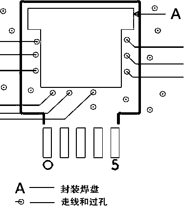
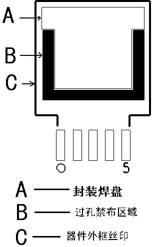
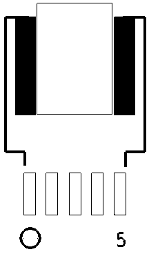
[0015] In this embodiment, the LDO device is taken as an example, such as figure 2 , 3 , the large pad at the bottom of the LDO is larger than its package pad, and a no-distribution area is set around the package pad to ensure that when there are traces and vias in this area, there will be a DRC error reminder, or it will not be possible directly. Holes are punched, so designers can avoid punching holes here. In this way, the risk of short circuit between the package pad and the via hole after soldering can be prevented, such as Figure 4 .

[0016] Using this method can improve the reliability of the product: the forbidden area can prevent the PCB from punching wrong signal lines and vias around the packaging pads of electronic components during the design process, and ensure that signal lines o...


PUM


Abstract

The invention discloses a method for solving short circuit of a signal through hole and a packaging bonding pad. An electronic component is connected on a PCB (Printed Circuit board), a large bonding pad at the bottom of the electronic component is equal to the packaging bonding pad in size, and a distribution prohibiting area at which a through hole is not allowed to be punched is arranged at the periphery of the packaging bonding pad of the electronic component. When the through hole is punched in the arranged distribution prohibiting area, errors are reported, or the through hole can not be punched, the risk of short circuit of the through hole and the packaging bonding pad of the electronic component can be prevented, and the method is suitable for the design of all the bonding pad components.

Description

[0001] technical field [0002] The invention relates to the field of PCB application design, and more specifically, relates to a method for solving the short circuit between a signal via hole and an electronic component packaging pad. Background technique [0003] PCB (Printed Circuit Board), the Chinese name is printed circuit board, also known as printed circuit board, printed circuit board, is an important electronic component, a support for electronic components, and a provider of electrical connections for electronic components. Electronic components are the basic components applied to the PCB board. [0004] like figure 1 As shown, the conventional design for punching holes for LDO (LOW DROP-OUT-linear voltage regulator) and PCB traces, without any design processing around the large pad of the LDO, the via hole can be punched around the large pad of the LDO device If the size of the exposed copper area on the device body is greater than or equal to the large pad of ...

Claims


Application Information

Patent Timeline
Patent Type & Authority Applications(China)
IPC IPC(8): H05K1/02H05K1/11
Inventor 刘海龙周丽
Owner GUANGDONG VTRON TECH CO LTD
Why Eureka
Try Eureka