Methods of forming semiconductor films including I2-II-IV-VI4 and I2-(II,IV)-IV-VI4 semiconductor films and electronic devices including the semiconductor films

A semiconductor and conductive material technology, applied in semiconductor devices, semiconductor/solid-state device manufacturing, circuits, etc., can solve problems such as liver toxicity and carcinogenicity, limited desirability, hydrazine flammability, etc.

Inactive Publication Date: 2014-03-19
UNIV OF WASHINGTON CENT FOR COMMERICIALIZATION
View PDF2 Cites 6 Cited by
  • Summary
  • Abstract
  • Description
  • Claims
  • Application Information

AI Technical Summary

Problems solved by technology

Although this approach has improved resulting device efficiencies, hydrazine is flamm...

Method used


Image

  • Methods of forming semiconductor films including I2-II-IV-VI4 and I2-(II,IV)-IV-VI4 semiconductor films and electronic devices including the semiconductor films
  • Methods of forming semiconductor films including I2-II-IV-VI4 and I2-(II,IV)-IV-VI4 semiconductor films and electronic devices including the semiconductor films
  • Methods of forming semiconductor films including I2-II-IV-VI4 and I2-(II,IV)-IV-VI4 semiconductor films and electronic devices including the semiconductor films

Examples


example

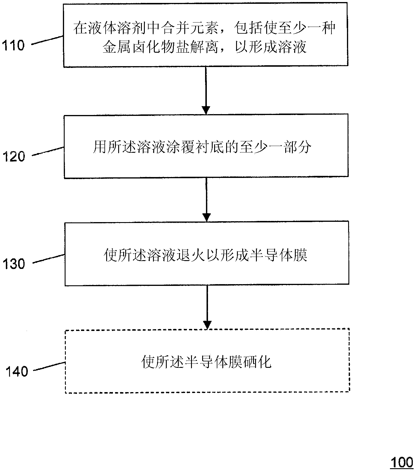
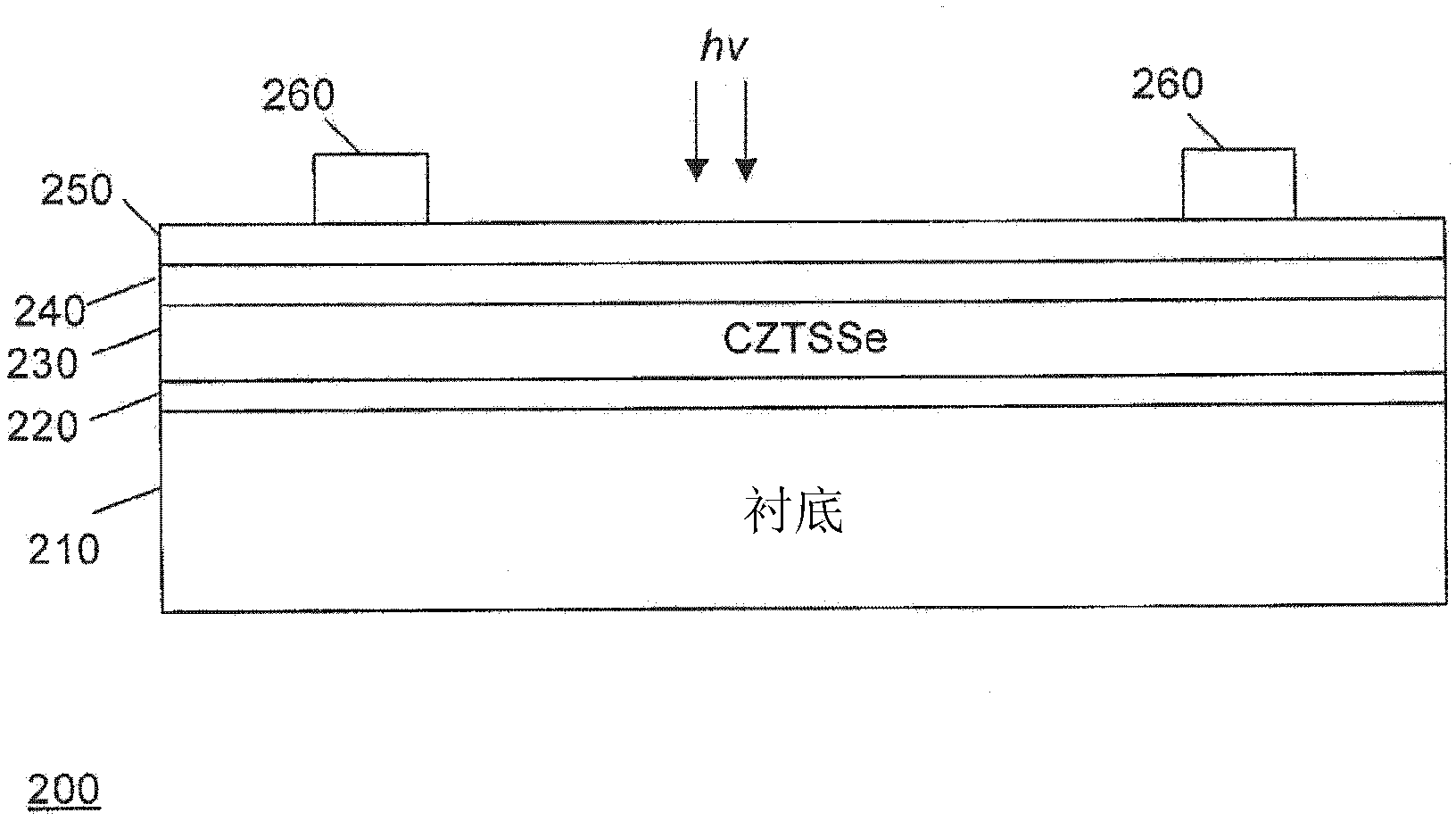
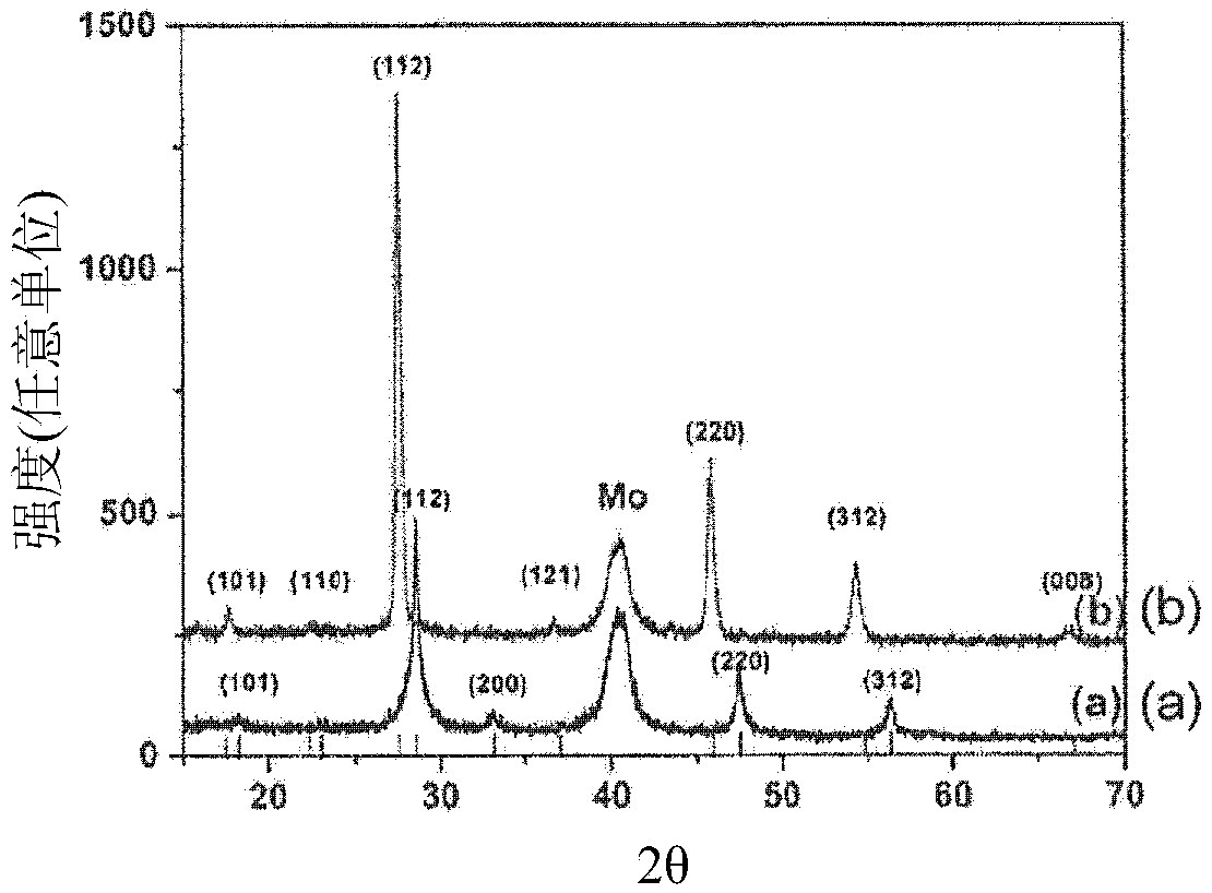
[0064] Examples of fabricating semiconductor films and electronic devices according to embodiments of the present invention are described below, and some experimental results are presented. It will be apparent to those skilled in the art that various modifications can be made in both materials and methods without departing from the scope of the invention.

[0065] Formation of semiconductor film

[0066] The coating solution to form the CZTS film was prepared by the following method: at room temperature, 0.8 mmol Cu(CH 3 COO)2 ·H 2 O (99.99%, obtained from Aldrich), 0.56 mmol ZnCl2 (99.1%, obtained from Mallinckrodt Baker), 0.55 mmol SnCl 2 .2H 2 O (99.995%, obtained from Aldrich) and 2.64 mmol thiourea (99%, obtained from Aldrich) were dissolved in 0.7 mL of dimethyl sulfoxide (DMSO) (99%, obtained from Aldrich). CZTS films were obtained by spin-coating the coating solution on Mo / SLG substrates followed by annealing at 580 °C on a hot plate. Spin coating was performed at...


PUM


Abstract

Embodiments of the present invention generally include methods for forming semiconductor films having nominal I2-II-IV-VI4 stoichiometry, such as CZTS or CZTSSe, using a solution of including sources of the I, II, IV, and VI elements in a liquid solvent. Precursors may be mixed in the solvent to form the solution. Metal halide salts may be used as precursors in some examples. The solution may be coated onto a substrate and annealed to yield the semiconductor film. In some examples, the source of the 'I' and 'IV' elements may contain the elements in a +2 oxidation state, while the semiconductor film may contain the 'I' element in a +1 oxidation state and the 'IV' element in a +4 oxidation state. Examples may be used to provide I2-(II,IV)-IV-VI4 films.

Description

[0001] Related Application Cross Reference [0002] This application claims priority to the filing date of US Provisional Application 61 / 444,398, filed February 18, 2011, which is incorporated herein by reference in its entirety. technical field [0003] Examples described herein may relate to methods of making semiconducting materials, compositions of semiconducting materials, and devices comprising such semiconducting materials. Semiconductor materials described herein include those with nominal I 2 -II-IV-VI 4 Stoichiometric thin films, including (but not limited to) CZTS or CZTSSe (such as Cu 2 ZnSnS 4 or Cu 2 ZnSn(S,Se) 4 ) film. Background technique [0004] Thin film semiconductor materials are useful in a variety of applications, including photovoltaic (PV) devices. CuInGaSe 2 (CIGSe) and CdTe to fabricate thin-film solar cells with suitable efficiencies. However, price volatility issues (eg, for In and Ga), abundance issues (for In and Te, which are rare e...

Claims


Application Information

Patent Timeline
IPC IPC(8): H01L31/032H01L31/18
CPCH01L31/18H01L21/02557H01L21/02491H01L31/072H01L31/0326H01L21/02568H01L21/02628H01L21/02422Y02E10/50H01L21/0256Y02E10/541Y02P70/50
Inventor 休·希尔豪斯纪佑锡
Owner UNIV OF WASHINGTON CENT FOR COMMERICIALIZATION
Why Eureka
Try Eureka