Micromechanical sensor device with movable gate and corresponding production method

A technology of micromechanical sensors and gates, applied in the direction of microstructure devices composed of deformable elements, microstructure devices, manufacturing microstructure devices, etc., to achieve the effects of reducing leakage current, improving SNR, and reducing thermal noise

Inactive Publication Date: 2014-03-26
ROBERT BOSCH GMBH
View PDF10 Cites 1 Cited by
  • Summary
  • Abstract
  • Description
  • Claims
  • Application Information

AI Technical Summary

Problems solved by technology

This increased noise can be largely attributed to parasitic leakage current

Method used


Image

  • Micromechanical sensor device with movable gate and corresponding production method
  • Micromechanical sensor device with movable gate and corresponding production method
  • Micromechanical sensor device with movable gate and corresponding production method

Examples


Embodiment Construction

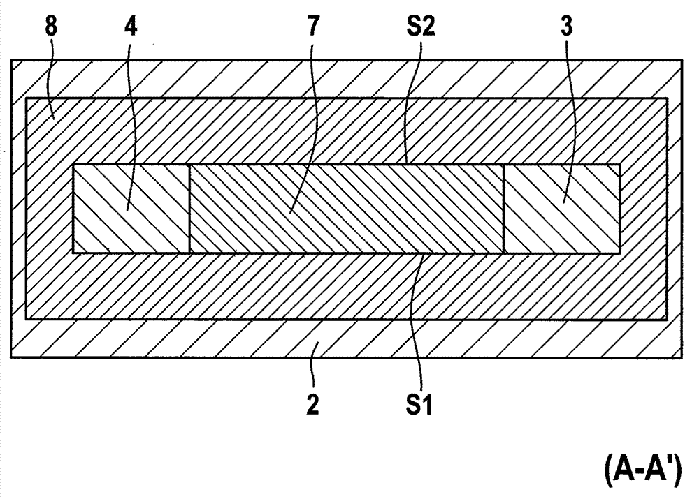
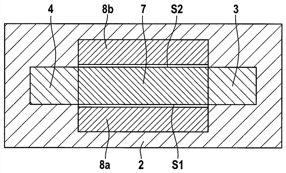
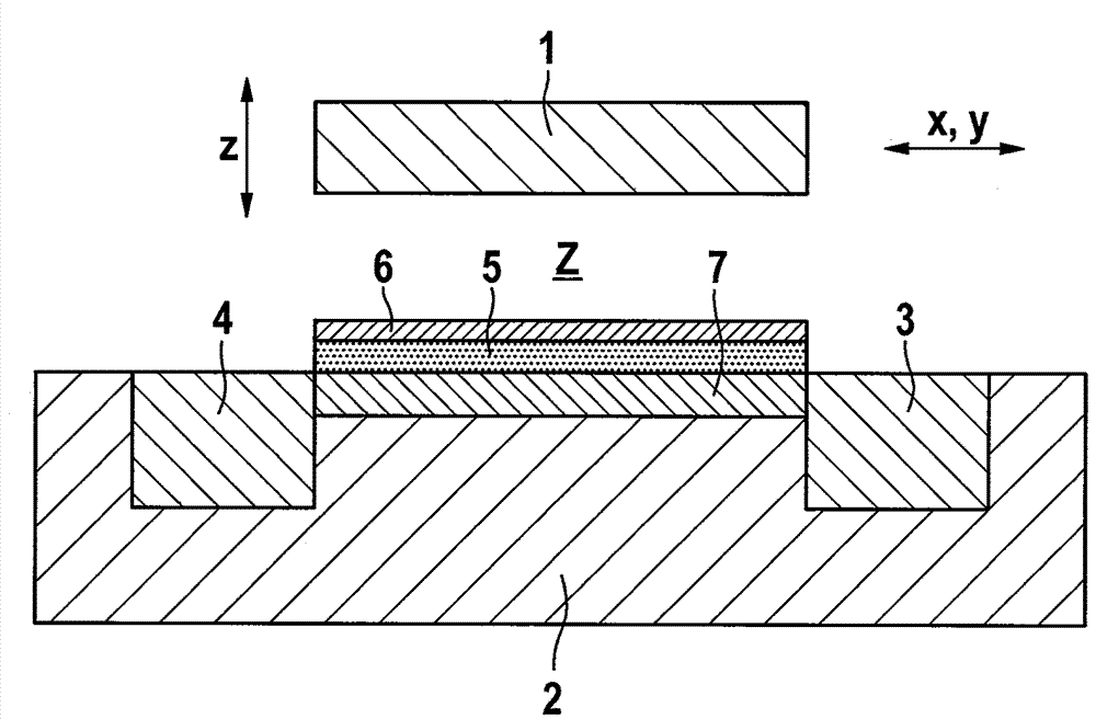
[0021] 1 a ) and 1 b ) are schematic cross-sectional views for illustrating a micromechanical sensor device with movable gates and a corresponding manufacturing method according to an embodiment of the invention, more precisely 1 a ) is a vertical cross-sectional view and FIG. 1 b ) is a horizontal cross-sectional view along line AA' in FIG. 1 a ).

[0022] In FIG. 1 a ) and FIG. 1 b ), the reference numeral 2 designates the silicon substrate in which the drain region 3 , the source region 4 and the channel region 7 in between of the field effect transistor are arranged. A gate insulating layer 5 , for example an oxide layer, is arranged on the channel region 7 . The surface charges on the insulating layer 5 are indicated with reference numeral 6 . The movable gate electrodes 1 are movably arranged on the base body 2 separated by a gap Z.

[0023] different from according to image 3 The above-mentioned known micromechanical sensor device, the embodiment of the invention has...


PUM

PropertyMeasurementUnit
depthaaaaaaaaaa

Abstract

The present invention realizes a micromechanical sensor device with a movable gate and a corresponding production method. The micromechanical sensor device with the movable gate includes a field effect transistor having a drain region (3), a source region (4), a channel region (7) arranged between the field effect transistor and the source region and including a first doping type, and a movable gate (1). The movable gate is separated from the channel region (7) by an interspace (Z). The drain region (3), the source region (4), and the channel region (7) are arranged in a substrate (2). An oxide region (8; 8a; 8b) is provided in the substrate (2) at least at longitudinal sides (S1, S2) of the channel region (7).

Description

technical field [0001] The invention relates to a micromechanical sensor arrangement with a movable gate and a corresponding production method. Background technique [0002] Although any desired micromechanical components are also applicable, the invention and the technical problems involved are explained on the basis of silicon-based components. [0003] Document DE 44 45 553 A1 describes a semiconductor acceleration sensor with a semiconductor body, a carrier structure supported by the semiconductor body and with fixed electrodes, the carrier structure having movable electrodes arranged on the semiconductor substrate. The sensor section is formed by the movable electrode and the fixed electrode and is accelerated by a change in current between the fixed electrodes, which is accompanied by a change in current of the movable electrode Acceleration acts on the sensor section to cause deflection. [0004] Document EP 0 990 911 A1 describes a micromechanical sensor based on ...

Claims


Application Information

Patent Timeline
Patent Type & Authority Applications(China)
IPC IPC(8): B81B7/00B81B7/02B81C1/00
CPCB81B3/0086B81B3/00B81C1/00H01L29/84B81B3/0018B81C1/00134
Inventor O.雅科夫莱夫A.布曼A.法伊
Owner ROBERT BOSCH GMBH
Why Eureka
Try Eureka