Signal processing circuit, image sensor IC, and signal processing method

a signal processing circuit and image sensor technology, applied in the field of signal processing circuits, can solve the problems of increasing the number of constituent elements, amplifiers are also amplified, circuits of amplifier chips cannot cope, etc., and achieve the effects of reducing thermal noise of reference voltage, reducing dispersion of ics, and large capacity

Active Publication Date: 2007-03-13
ABLIC INC
View PDF9 Cites 12 Cited by
  • Summary
  • Abstract
  • Description
  • Claims
  • Application Information

AI Technical Summary

Benefits of technology

[0027]In accordance with this image sensor, since the reset voltages of the photodiodes of all the image sensor ICs become identical to one another, it is possible to reduce a dispersion in sensitivity among the ICs. Also, a capacitor having a large capacity is inserted between the reference voltage terminal made common to the image sensor ICs and the GND terminal or the like to reduce the thermal noises of the reference voltage, whereby it is possible to solve the problem in that steaks are formed in a read-out image.
[0028]As described above, according to the present invention, it is possible to obtain the photoelectric converter which is small in fixed pattern noise. Consequently, it is possible to supply the image sensor IC which is simple in configuration and which is small in dispersion of the dark output signals.
[0029]In addition, in a case of manufacturing a close contact type image sensor in which a plurality of image sensor ICs described above are linearly mounted, it is possible to reduce a difference in level among chips.
[0030]Also, dispersion in sensitivity among ICs can be reduced with a simple configuration. Moreover, it is possible to solve the problem in that streaks are formed in a read-out image.

Problems solved by technology

However, the image sensor of Related Art Example 1 has a disadvantage that the amplifier chip 200 and the sensor chip 100 need to be provided separately from each other, thereby increasing the number of constituent elements.
In addition, there arises a problem in that the circuit of the amplifier chip cannot cope with a sensor chip of such a type as to be adapted to output the reference signal and the optical signal to the same common signal line in order.
Moreover, there also arises a problem in that if the image sensor is provided with an amplification function, then an offset of the amplifier is also amplified.
In addition, the image sensor of Related Art Example 2 has a problem in that if a difference between the voltage of VREF3 and the voltage appearing at the terminal 106 is large, then a level of the output signal of the inversion amplifier D is easy to be beyond an output range.
Thus, it is difficult to ensure a linear area having broad photoelectric conversion characteristics for outputs of all bits.
That is, there arises a problem in that since the different reset noises of the timings are compared with each other, a random noise becomes large.
However, practically, since a capacitor having a large capacity cannot be provided inside an IC, it is difficult to reduce these thermal noises.
Consequently, there arises a problem in that a signal level is changed every read line, and hence streaks are formed in a read-out image.
In addition, there also arises a problem in that since the reset voltages of the image sensor ICs are different from one another and hence a reverse bias voltage of the photodiode differs every IC, a sensitivity varies among ICs.

Method used


Image

  • Signal processing circuit, image sensor IC, and signal processing method
  • Signal processing circuit, image sensor IC, and signal processing method
  • Signal processing circuit, image sensor IC, and signal processing method

Examples


first embodiment

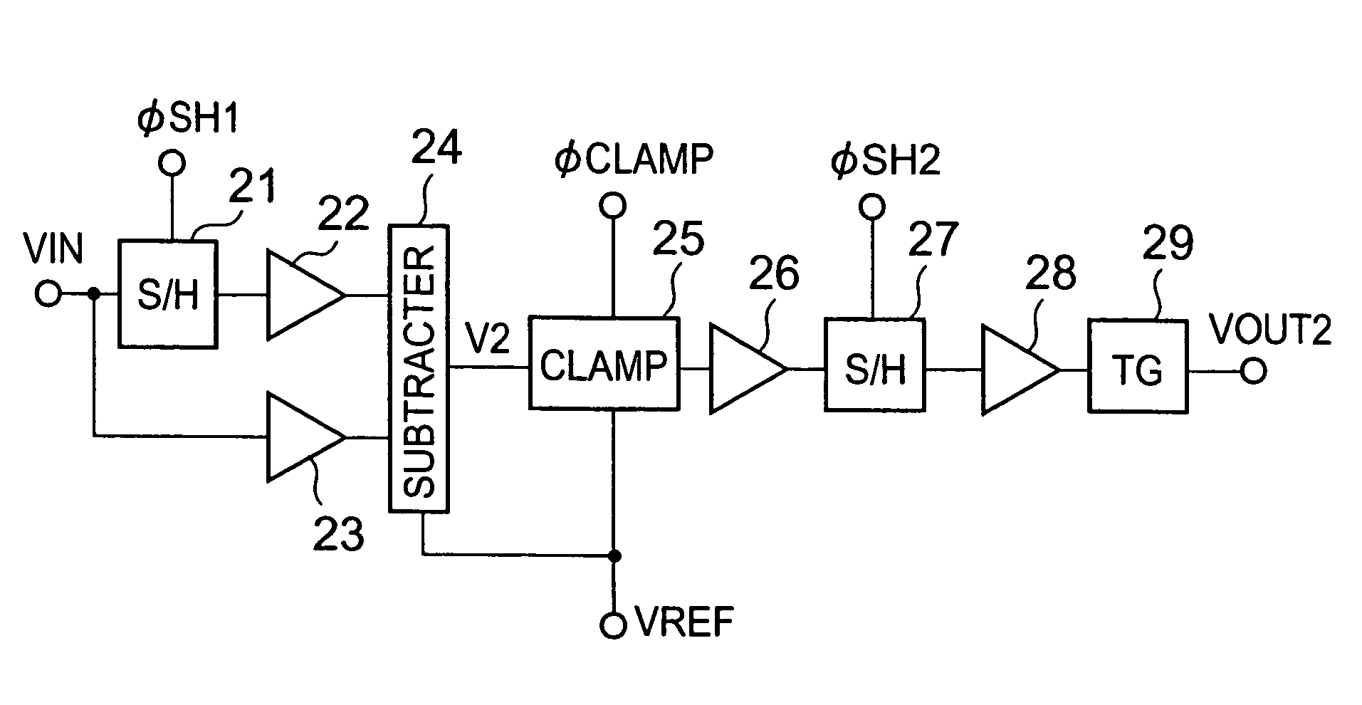
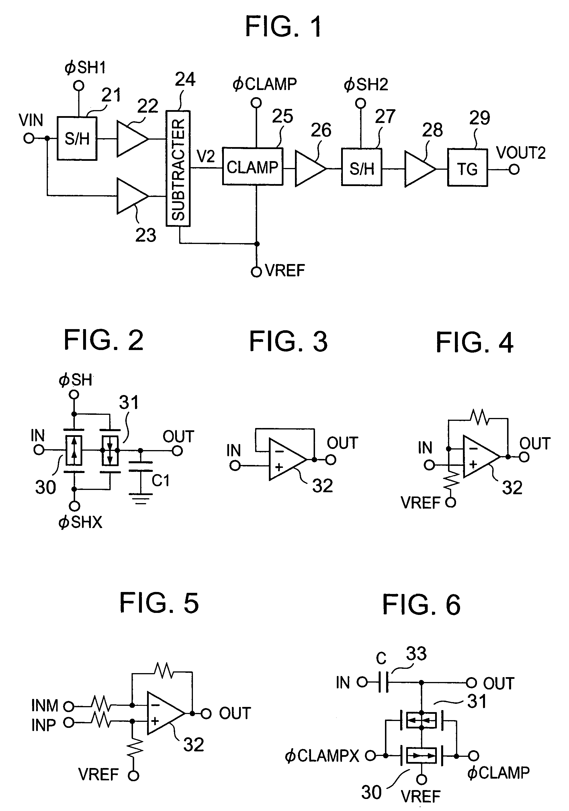
[0055]FIG. 1 is a block diagram of a signal processing circuit according to a first embodiment of the present invention. A signal is inputted to a sample / hold circuit 21 and a buffer amplifier 23 through an input terminal VIN. An output signal of the sample / hold circuit 21 is inputted to a buffer amplifier 22. An output signal of the buffer amplifier 22 and an output signal of the buffer amplifier 23 are inputted to a subtracter 24, an output signal of which is in turn inputted to a voltage clamp circuit 25. A reference voltage for the subtracter 24 and a reference voltage for the voltage clamp circuit 25 can be made common to each other. Then, respective terminals of the subtracter 24 and the voltage clamp circuit 25 are connected to a terminal VREF. An output signal of the voltage clamp circuit 25 is inputted to a buffer amplifier 26. Note that the buffer amplifier 26 may be replaced with an amplification circuit. Moreover, a terminal at which a reference voltage for this amplific...

second embodiment

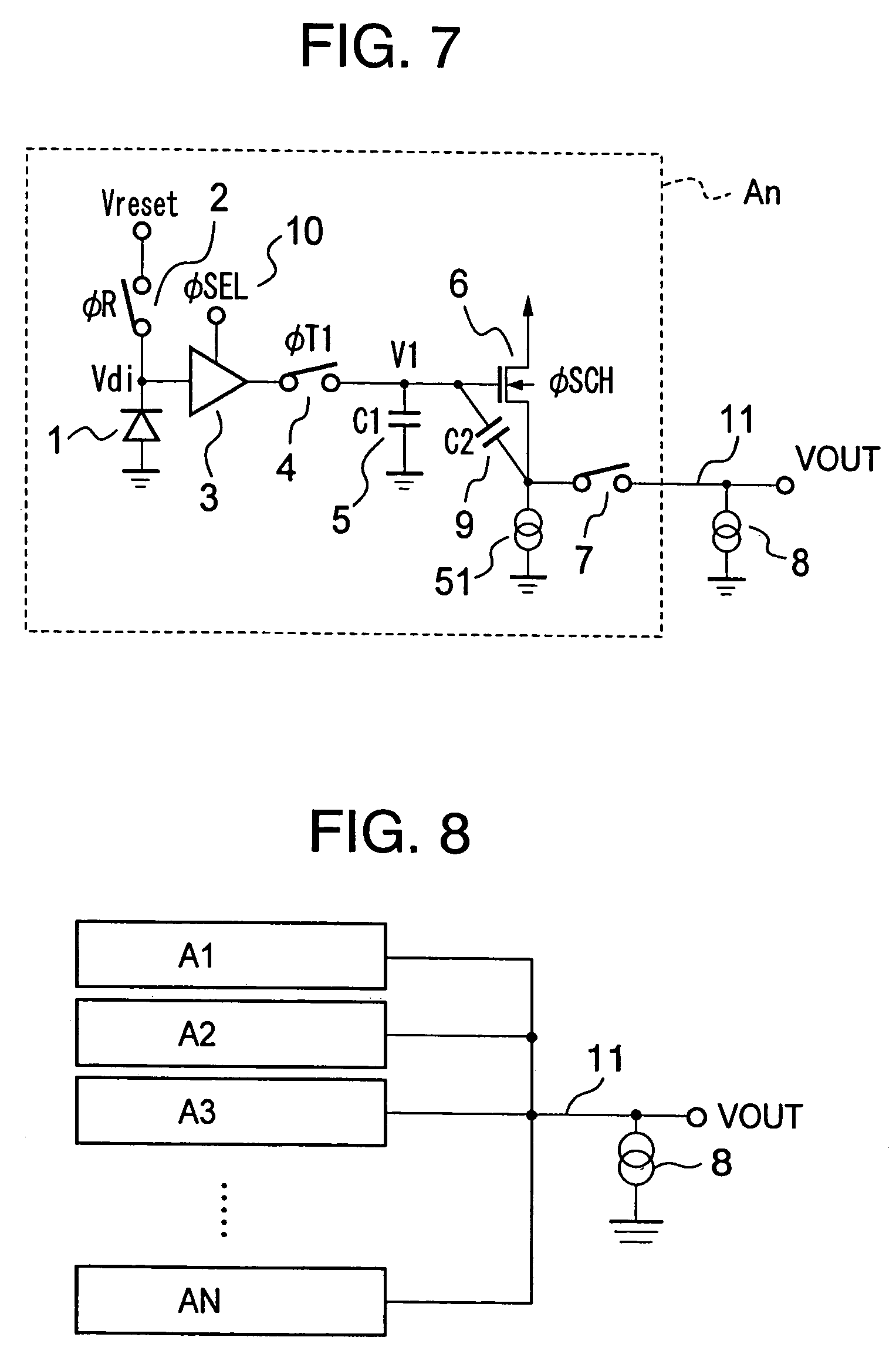
[0077]FIG. 10 is a schematic circuit diagram of a photoelectric converter according to a second embodiment of the present invention. The number of sets of constituent elements provided inside a frame of a photoelectric conversion block An shown in FIG. 10 is identical to the number of pixels. A channel selection switch 7 of each block is connected to a common signal line 11. Note that the photoelectric conversion block An shows a photoelectric conversion block of an n-th bit. A diagram of a configuration of the whole photoelectric converter is shown in FIG. 8. The configuration is the same as that in the first embodiment of the present invention.

[0078]The circuit of the photoelectric conversion block An includes: a photodiode 1 serving as a photoelectric conversion unit; transfer switches 14, 15, 16, and 17 serving as an electric charge transfer unit; a reset switch 2 serving as a reset unit; an amplification unit 3; a capacitor 13 for holding an optical signal; a capacitor 12 for h...

third embodiment

[0092]FIG. 12 is a schematic diagram of a close contact type image sensor according to a third embodiment of the present invention. This close contact type image sensor includes three image sensor ICs 41. Each image sensor IC 41 includes a signal processing circuit 42, a photoelectric converter 43, a reference voltage circuit 44, a resistor 45, a reference voltage terminal 46, and a signal output terminal 47. A common signal line of the photoelectric converter 43 is connected to the signal processing circuit 42, and an output terminal of the signal processing circuit 42 is connected to the signal output terminal 47. In addition, a reference voltage of the signal processing circuit 42 appears at the reference voltage terminal 46, and a resistor 45 is provided between the reference voltage circuit 44 and the reference voltage terminal 46.

[0093]The signal output terminals 47 of all the image sensor ICs 41 are connected to one another in the outside, and output signals of all the image ...


PUM


Abstract

A signal processing circuit has a sample/hold circuit for sampling an input signal comprised of a first signal and a second signal and for holding the first signal. The first signal comprises an optical signal obtained due to storage of electric charges generated due to light incident upon a photoelectric converter, and the second signal comprises a reference signal obtained due to resetting of the photoelectric converter. A subtracter receives an output signal of the sample/hold circuit and the input signal and obtains a difference between the output signal of the sample/hold circuit and the input signal. A voltage clamp circuit clamps a part or all of an output signal from the subtracter.

Description

BACKGROUND OF THE INVENTION[0001]1. Field of the Invention[0002]The present invention relates in general to a signal processing circuit, such as an image sensor, for processing an analog signal. In addition, the invention relates to a linear image sensor and an area image sensor each of which is loaded with the signal processing circuit. Also, the invention relates to a close contact type image sensor having a plurality of linear image sensor ICs mounted thereto.[0003]2. Related Background Art[0004]A circuit diagram of an image sensor of Related Art Example 1 is shown in FIG. 19, and a timing chart of the image sensor of Related Art Example 1 is shown in FIG. 20 (refer to JP 11-112015 A (page 4 and page 5, and FIG. 1) for example).[0005]Related Art example 1 aims at providing a high performance close contact type image sensor which requires no dark correction through removal of an FPN (Fixed Pattern Noise) due to a difference in level among chips.[0006]In accordance with Related Art...

Claims


Application Information

Patent Timeline
Patent Type & Authority Patents(United States)
IPC IPC(8): H01L27/00G06T1/00H01L27/146H04N1/028H04N1/19H04N5/335H04N5/365H04N5/378
CPCH04N5/3575H04N5/3658H04N5/3653H04N5/363H01L27/146H04N25/616H04N25/65H04N25/672H04N25/677
Inventor MACHIDA, SATOSHI
Owner ABLIC INC
Why Eureka
Try Eureka