Anti-static display panel

A display panel, anti-static technology, applied in instruments, nonlinear optics, optics, etc., can solve the problem that the static electricity of the thin film transistor substrate cannot be effectively discharged, and achieve the effect of avoiding abnormal display.

Active Publication Date: 2014-03-26
SHANGHAI AVIC OPTOELECTRONICS
View PDF5 Cites 18 Cited by
  • Summary
  • Abstract
  • Description
  • Claims
  • Application Information

AI Technical Summary

Problems solved by technology

This method reduces the change of the potential of the common electrode when there is static electricity, but the static electricity of the thin film transistor substrate itself still cannot be effectively released

Method used


Image

  • Anti-static display panel
  • Anti-static display panel
  • Anti-static display panel

Examples


Embodiment 1

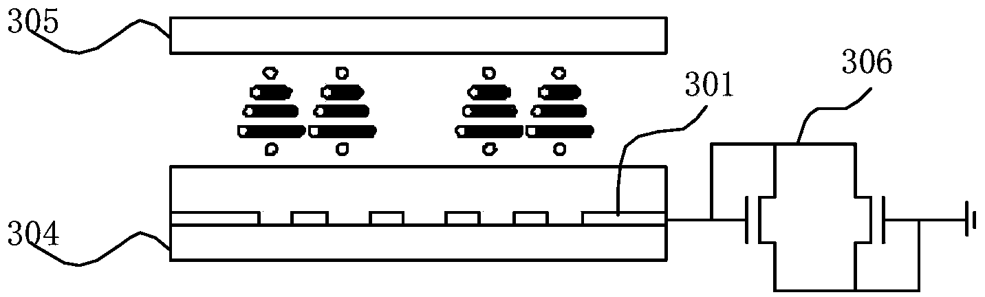
[0046] Such as image 3 As shown, a thin film transistor liquid crystal display panel provided in Embodiment 1 of the present invention includes: a TFT substrate 304, a CF substrate 305, a liquid crystal disposed between the TFT substrate and the CF substrate, and the liquid crystal display panel includes a display area and a non-display area, the non-display area is arranged around the display area, and the common electrode 301 surrounding the display area is arranged in the non-display area.

[0047] It also includes: an electrostatic protection device (ESD device) 306, one end of which is connected to the common electrode 301, and the other end is grounded.

[0048] The electrostatic protection device 306 can be one-stage, two-stage or multi-stage.

[0049] Preferably, the electrostatic protection device 306 is one-stage or two-stage.

[0050] Figure 4 with Figure 5 It is a schematic circuit diagram of a one-level and two-level ESD protection device. Figure 4 The el...

Embodiment 2

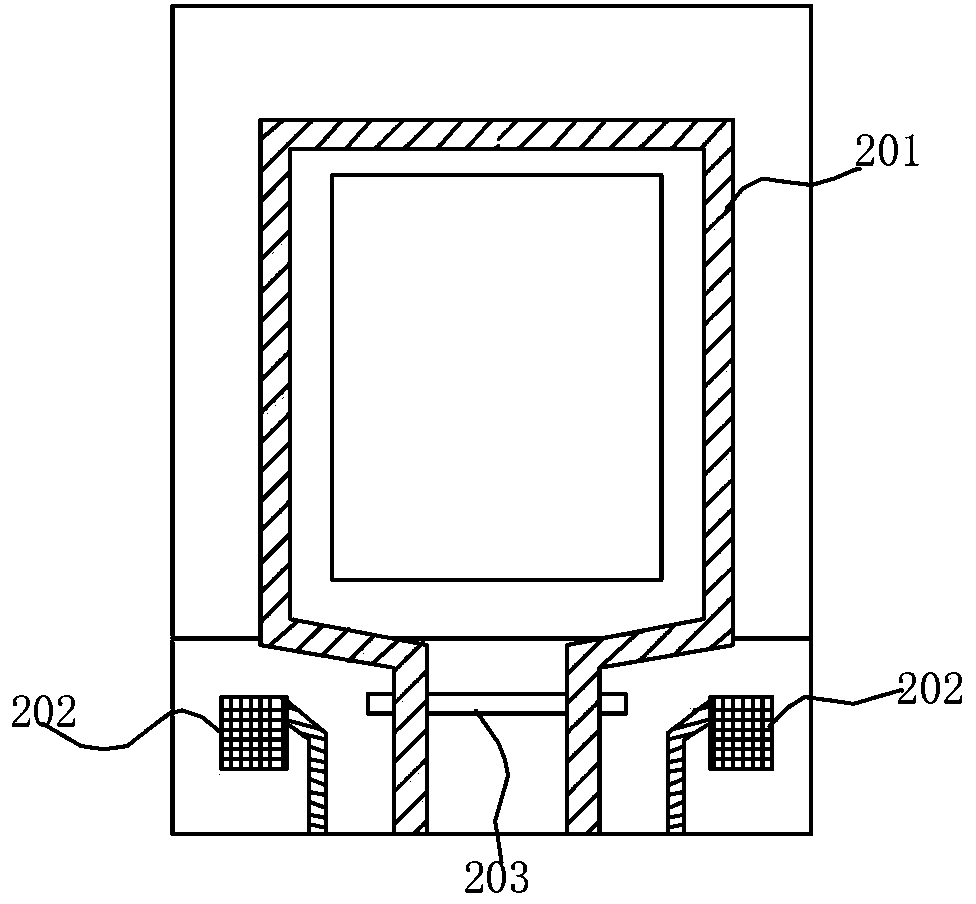
[0055] Such as Figure 6 As shown, the thin film transistor substrate provided by the second embodiment of the present invention at least includes a display area AA, and a non-display area surrounding the display area AA; in the non-display area, a display area surrounding the thin film transistor substrate is provided An ESD device 606 is also provided in the non-display area; the common electrode 601 is connected to one end of the ESD device 606; a ground connection around the display area of ​​the thin film transistor substrate is also provided in the non-display area The protection ring 607; the other end of the ESD device 606 is connected to the protection ring 607.

[0056] The material of the protection ring 607 is metal.

[0057] The guard loop potential of the guard loop 607 is provided by a peripheral driving circuit.

[0058] At least two ends of the protection loop 607 are grounded.

[0059] In the above-mentioned thin film transistor liquid crystal display pane...

Embodiment 3

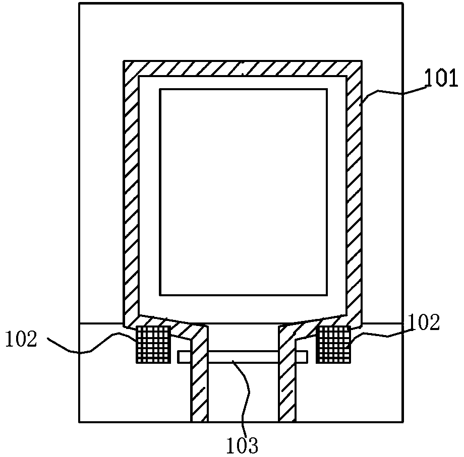
[0062] As shown in FIG. 7( a ), Embodiment 3 of the present invention provides an IPS-LCD display panel, including: a TFT substrate 704 , a CF substrate 705 , and liquid crystal disposed between the TFT substrate and the CF substrate. A transparent conductive layer 708 is disposed on the CF substrate.

[0063] As shown in FIG. 7( b ), the TFT substrate 704 includes a display area AA and a non-display area, and the non-display area surrounds the display area AA.

[0064] The common electrode 701 is disposed in the non-display area and surrounds the display area AA. An ESD device 706 is arranged in the non-display area; the common electrode 701 is connected to one end of the ESD device 706; a grounded protection loop 707 is also arranged in the non-display area, and the protection loop 707 surrounds the The display area; the other end of the ESD device 706 is connected to the protection ring 707. At least one conductive pad 702 is arranged on the guard ring 707 . The conducti...


PUM


Abstract

The invention discloses an anti-static display panel. The anti-static display panel comprises a thin film transistor base plate which comprises at least one display area, common electrodes arranged around the at least one display area of the thin film transistor base plate and an electronic static discharge (ESD) device, wherein one end of the ESD device is connected with the common electrodes, and the other end of the ESD device is grounded. The invention further discloses a grounded protection loop circuit which is arranged on the periphery of the at least one display area of the thin film transistor base plate. One end of the ESD device is connected with the common electrodes, and the other end of the ESD device is connected with the grounded protection loop circuit. The anti-static display panel can release static electricity on the common electrodes, and avoids the problem that a driver chip can not normally display due to self protection.

Description

technical field [0001] The invention relates to the technical field of liquid crystal display, in particular to an electrostatic protection circuit. [0002] Background technique [0003] In recent years, various display panels are widely used in both information communication equipment and general electrical equipment. [0004] As a flat panel display device, a liquid crystal display usually includes an upper substrate, a lower substrate and a liquid crystal layer between the two substrates. Usually, the lower substrate is integrated with several data lines and scan lines, which are vertically interlaced to form several unit areas, and these unit areas are defined as pixel units. Each pixel unit mainly includes components such as a pixel electrode, a storage capacitor, and a thin film transistor (TFT). The driving circuit provides driving signals to the scanning lines to control the working state of the thin film transistors, so as to timely write the driving signals pr...

Claims


Application Information

Patent Timeline
IPC IPC(8): G02F1/1343G02F1/1362G02F1/1335
Inventor 岳明彦
Owner SHANGHAI AVIC OPTOELECTRONICS
Why Eureka
Try Eureka