
Thin film transistor (TFT) array substrate and liquid crystal panel thereof

A technology for array substrates and liquid crystal panels, applied in the field of TFT array substrates and liquid crystal panels, can solve problems such as unclean etching, short-circuiting of short-circuit bars, abnormal display of substrates, etc., and achieve the effect of avoiding abnormal display problems

Active Publication Date: 2014-03-26
SHANGHAI AVIC OPTOELECTRONICS
View PDF5 Cites 13 Cited by
  • Summary
  • Abstract
  • Description
  • Claims
  • Application Information

AI Technical Summary

Problems solved by technology

[0003] However, in the manufacturing process of the array substrate, the produced shorting bars may be short-circuited with each other.
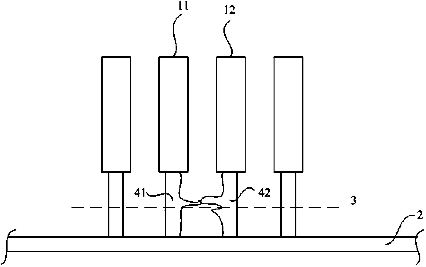
Taking ITO (Indium Tin Oxide) as the material for making shorting bars as an example, if there is residual ITO etching, there will still be a short circuit phenomenon between the shorting bars after cutting, so in the testing stage, since each shorting bar is connected to There is a risk of short circuit between two adjacent pads, and the result will cause abnormal display of the substrate or even failure to light up during the test.
like figure 2 As shown, two adjacent pads 11, 12 respectively correspond to shorting bars 41, 42, because the etching is not clean, after cutting along the cutting line 3, although pad11 and pad12 are no longer commonly connected to the shorting ring 2, but They are still shorted to each other

Method used


Image

  • Thin film transistor (TFT) array substrate and liquid crystal panel thereof
  • Thin film transistor (TFT) array substrate and liquid crystal panel thereof
  • Thin film transistor (TFT) array substrate and liquid crystal panel thereof

Examples


Embodiment 1

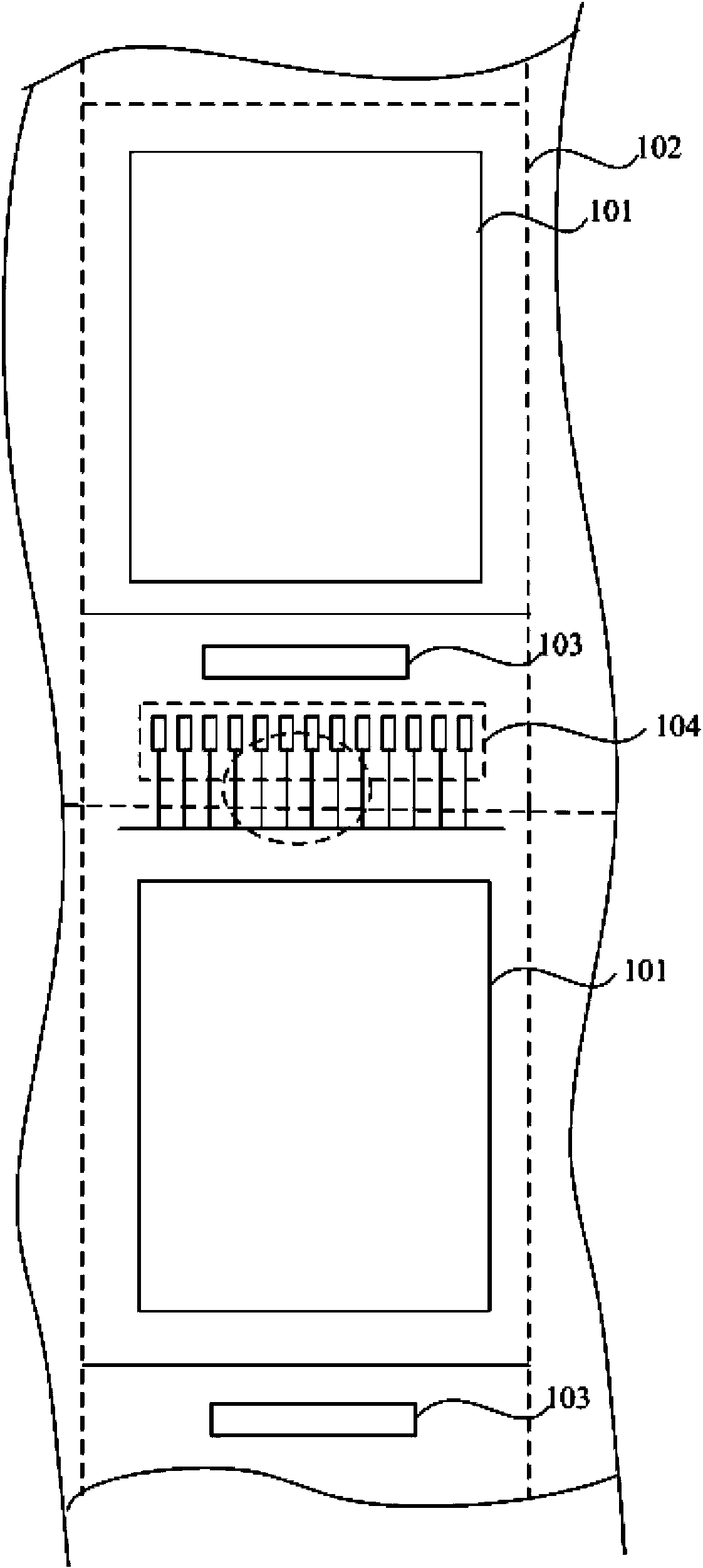
[0054] see image 3 and Figure 4 . in, image 3A TFT array substrate provided by the present invention is shown, and the array substrate 102 includes a display area 101 and a non-display area other than the display area 101 . The non-display area includes an IC (Integrated Circuit) driver chip 103, which is used to transmit various received signals to the array substrate to control the gray scale of the display; the pad area 104 is used to receive external signals, and transmit the The signal is correspondingly transmitted to the IC driver chip; and other wires (not shown in the figure). Figure 4 yes image 3 A partially enlarged view of the pad region 104 at the edge of the array substrate 102 in .

[0055] refer to Figure 4 , the TFT array substrate of the present invention, comprising:

[0056] Substrate 1;

[0057] A plurality of pads 2 on the surface of the substrate 1, the pads 2 are used to receive external signals; the pads 2 here can be FOG pads, test p...

Embodiment 2

[0071] This embodiment is a further embodiment obtained on the basis of the first embodiment. see Figure 8 The difference between this embodiment and the first embodiment is that the liner 2 includes a first liner 21 and a second liner 22 . For the convenience of description, the first short-circuit bar 3 also includes a first sub-short-circuit bar 31 and a second sub-short-circuit bar 32 correspondingly, the first sub-short-circuit bar 31 is set correspondingly to the first pad 21, and the second sub-short-circuit bar 32 is connected to the second sub-short-circuit bar 32 . The two pads 22 are arranged correspondingly. Preferably, the first pad 21 is a FOG pad. Further, the second pad 22 is a test pad.

[0072] The ESD device 5 includes a first ESD device 51 and a second ESD device 52, the first ESD device 51 is electrically connected to the first pad 21 and the first sub-short bar 31 corresponding thereto, and the second ESD device 52 is electrically connected to the sec...

Embodiment 3

[0075] This embodiment is further obtained on the basis of the second embodiment. The difference from Embodiment 2 is that in this embodiment, since the FOG pad 21 is more susceptible to electrostatic hazards than the test pad 22, the first short circuit bar 31 electrically connecting the FOG pad 21 and the first sub-short bar 31 The ESD device 51 adopts a first-level bidirectional ESD device, which has played the role of faster discharge; the second ESD device 52 electrically connected to the test pad 22 and the second sub-short bar 32 adopts a multi-level ESD device, preferably, the second ESD device 52 uses two-stage bidirectional ESD devices.

[0076] see Figure 9 , Figure 9 is a schematic diagram of a TFT-based two-stage bidirectional ESD device. The two-stage bidirectional ESD device is formed by connecting two one-stage bidirectional ESD devices in series. see also Figure 8 , Figure 9 , the A terminal of the second ESD device 52 is electrically connected to th...


PUM


Abstract

The invention provides a thin film transistor (TFT) array substrate and a liquid crystal panel thereof. The TFT array substrate comprises a substrate, a plurality of gaskets, a plurality of first short-circuiting bars, second short-circuiting bars and a plurality of electronic static discharge (ESD) devices, wherein the gaskets are located on the surface of the substrate and used for receiving external signals, the first short-circuiting bars are located on the surface of the substrate and correspond to the gaskets, the second short-circuiting bars are located on the surface of the substrate to be connected with all the first short-circuiting bars, and the ESD devices are located on the surface of the substrate and electrically connected with the gaskets and the first short-circuiting bars corresponding to the gaskets. The problem of display abnormity caused by short circuiting between the short-circuiting bars and the corresponding gaskets caused by ITO etching uncleanness during testing is solved while an anti-static function in the array substrate manufacturing process is achieved.

Description

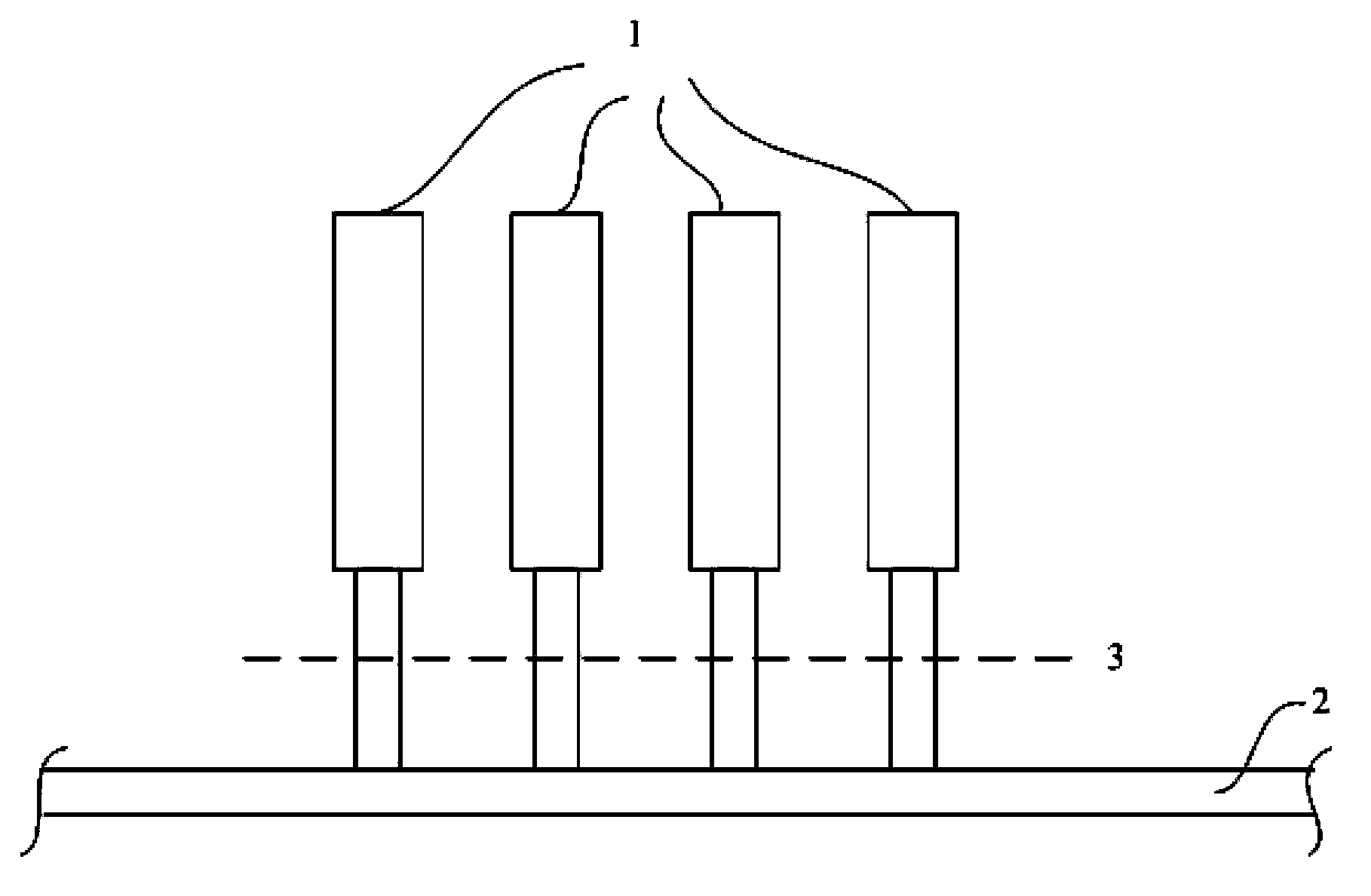
technical field [0001] The invention relates to the field of liquid crystal display, in particular to a TFT array substrate and a corresponding liquid crystal panel. Background technique [0002] In recent years, liquid crystal display panels are widely used in both information communication equipment and common electrical equipment. Static electricity is easy to accumulate during the production process of liquid crystal panels or array substrates, and if the static electricity problem cannot be solved well, it will easily cause serious damage to the product. For the FOG (flexible circuit board and glass circuit board connection device) pad (liner) and test pad in the manufacturing process of the array substrate, the traditional anti-static protection method is to prevent static electricity by connecting a short-circuit bar to form a short-circuit ring. Such as figure 1 As shown, 1 indicates a FOG pad or a test pad, and 2 indicates a short-circuit ring connected to all sho...

Claims


Application Information

Patent Timeline
Patent Type & Authority Applications(China)
IPC IPC(8): G02F1/1362G02F1/13H01L27/02
Inventor 岳明彦
Owner SHANGHAI AVIC OPTOELECTRONICS
Learn More