Laser simulation single particle effect back irradiation test method for memory circuit

A memory circuit, single-event effect technology, applied in static memory, instruments, etc., can solve problems such as difficulty in analyzing the influence of single-event performance, difficulty in obtaining pulsed laser response characteristics, difficulty in single-event sensitivity, etc., to reduce experimental errors. , The effect of simplifying the test steps and reducing the cost

Active Publication Date: 2014-03-26
BEIJING MXTRONICS CORP +1
View PDF2 Cites 22 Cited by
  • Summary
  • Abstract
  • Description
  • Claims
  • Application Information

AI Technical Summary

Problems solved by technology

The exact position of a specific functional unit cannot be found during backside irradiation, so it is difficult to obtain the pulse laser response characteristics of sensitive nodes in the circuit, and it is also difficult to analyze the influence of sensitive node layout factors of the circuit layout on the performance of single particles. The single-event sensitivity of the
When the laser is focused on the back surface during back irradiation, the spot will diverge and become larger when irradiating through the substrate of the device to the active area. Therefore, to obtain a small spot, the laser must be focused on the active area of ​​the device, which is different from the device substrate. Thickness is dependent, making testing difficult

Method used


Image

  • Laser simulation single particle effect back irradiation test method for memory circuit
  • Laser simulation single particle effect back irradiation test method for memory circuit
  • Laser simulation single particle effect back irradiation test method for memory circuit

Examples


Embodiment Construction

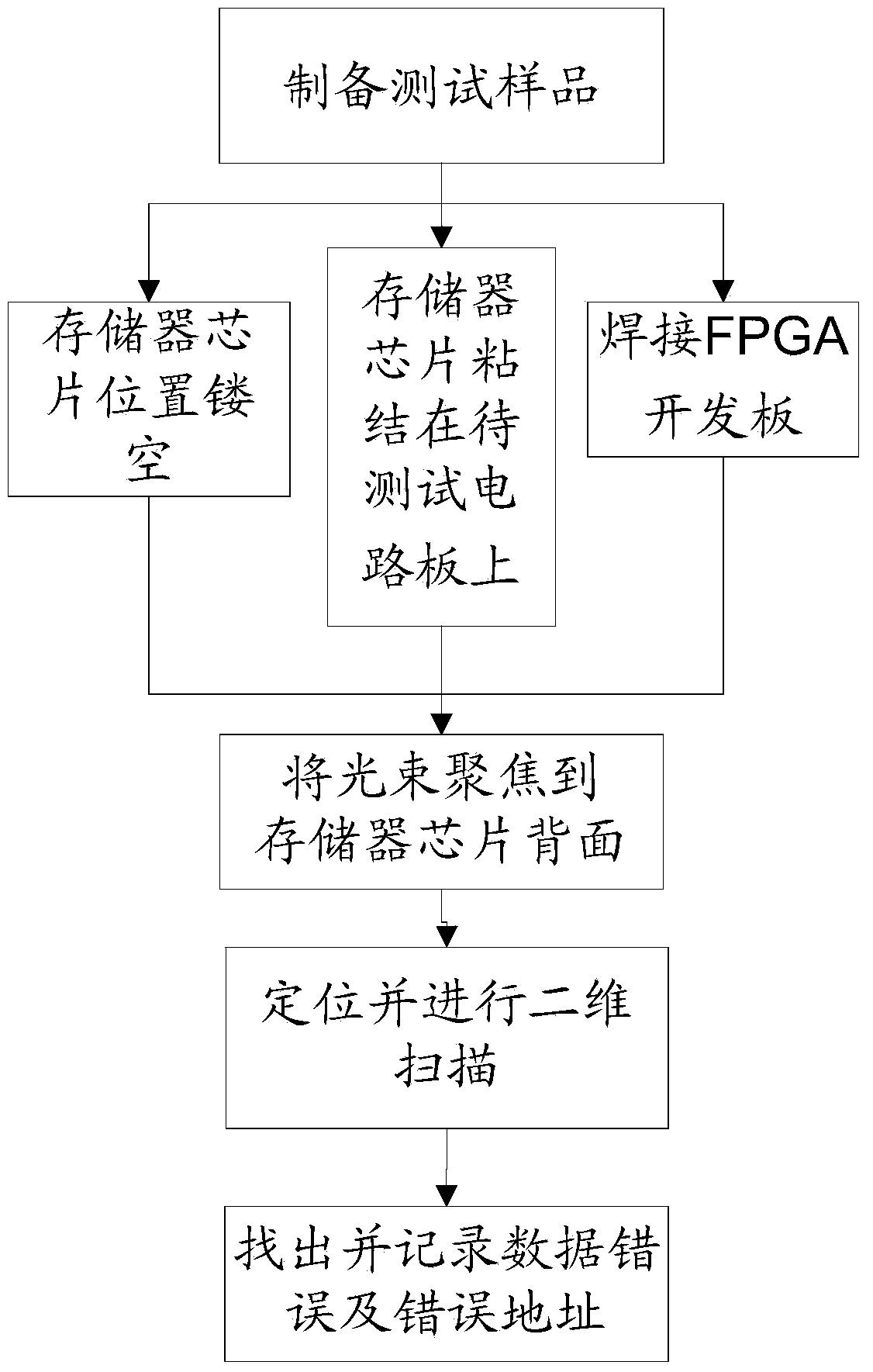
[0028] figure 1 The process flow of the pulsed laser simulation single event effect back irradiation test method for the memory circuit of the present invention is described:

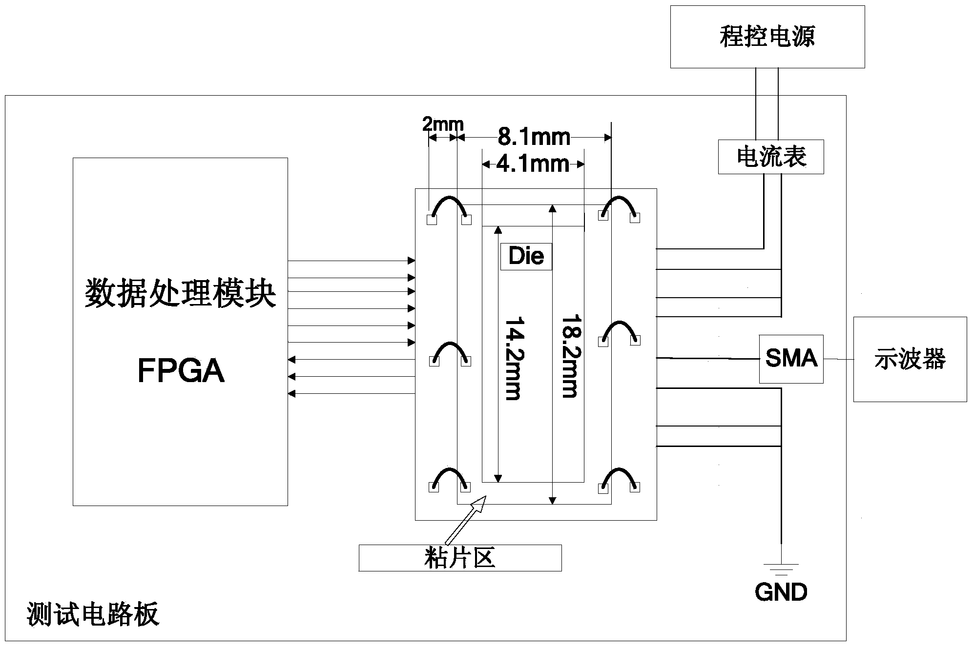
[0029] (1) Prepare memory circuit test samples; first, hollow out the position where the memory chip is bonded on the circuit board to be tested to form a hollow hole. The shape and size of the hollow hole are based on the shape and size of the memory chip, and a 2mm sticky chip is reserved around it area, and the rest of the central part is hollowed out; then the memory chip is bonded to the circuit board to be tested, and the memory chip is bonded to the pad of the circuit board to be tested with aluminum wire; at the same time, the FPGA development board is also soldered to the circuit board to be tested ;

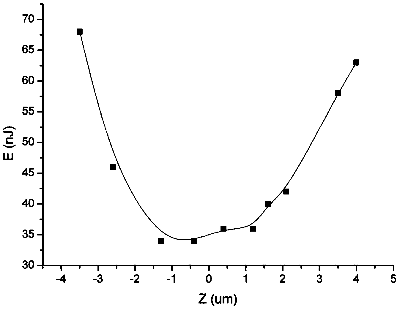
[0030] (2) Fix the memory circuit test sample on the three-dimensional translation stage, drive the three-dimensional translation stage, make the pulsed laser emitted by the external laser focus...


PUM


Abstract

The invention discloses a laser simulation single particle effect back irradiation test method for a memory circuit. The method comprises the following the steps: 1) hollowing the position at which a memory chip is adhered to a circuit board to be tested; 2) fixedly placing a memory circuit test sample on a three-dimensional translation platform, driving the three-dimensional translation platform, focusing pulse laser emitted from an external laser to the back surface of the memory chip after the pulse laser passes through a lens, and fixing the memory circuit test sample at the position in a vertical direction; 3) driving the three-dimensional platform to move, and scanning the memory circuit test sample in a two-dimensional plane; 4) monitoring the input and the output of the memory chip by using an FPGA (field programmable gate array), finding out and recording data errors and erroneous data addresses generated by data flip of the memory chip caused by the pulse laser. According to the method, the position of an error can be positioned accurately without an infrared camera.

Description

technical field [0001] The invention relates to a research and analysis method for the anti-space single event effect capability of semiconductor devices. Background technique [0002] Spacecraft are exposed to cosmic rays, particles in the Earth's radiation belt, and atmospheric neutrons in space. The total dose effect and single event effect will be produced when spaceborne devices are exposed to radiation. With the reduction of the feature size of the semiconductor process, the single event effect of the device becomes more and more significant. Carrying out the research and analysis of the single event effect of aerospace electronic devices is of great significance for prolonging the life of satellites and improving the reliability of integrated circuits. [0003] In order to ensure the safe and reliable flight of space vehicles, it is necessary to conduct ground simulation of single event effects on aerospace electronic devices to evaluate the performance of single ev...

Claims


Application Information

Patent Timeline
Patent Type & Authority Applications(China)
IPC IPC(8): G11C29/56
Inventor 陈茂鑫范隆董攀陈莉明郑宏超岳素格杜守刚马建华王煌伟文圣泉毕潇于春青
Owner BEIJING MXTRONICS CORP
Why Eureka
Try Eureka