

A Method for Restraining Threshold Voltage Drift of PMOS Devices
A threshold voltage drift and device technology, applied in semiconductor devices, semiconductor/solid-state device manufacturing, circuits, etc., can solve problems such as unfavorable device performance stability, metal ion contamination, and gate structure and morphology have a great influence, and reduce aggregation. risk, the effect of suppressing threshold voltage drift
- Summary
- Abstract
- Description
- Claims
- Application Information
AI Technical Summary
Problems solved by technology
Method used
Image

Examples
Embodiment Construction
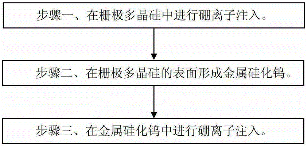
[0019] Such as image 3 Shown is the flow chart of the method of the embodiment of the present invention; the method for suppressing the threshold voltage drift of the PMOS device in the embodiment of the present invention includes the following steps:
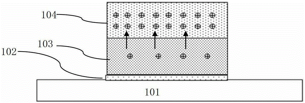
[0020] Step 1, such as Figure 4A As shown, a gate oxide layer 2 and a gate polysilicon 3 are sequentially formed on a silicon substrate 1. After the gate polysilicon 3 is formed, boron ion implantation is performed for the first time, and the first boron ion implantation implants boron ions into the gate polysilicon and make the gate polysilicon a P-type doped structure. The implantation energy of the first boron ion implantation is 3KeV-8KeV, and the implantation dose is 1E14cm -2 ~1E16cm -2 .
[0021] Step two, such as Figure 4A As shown, metal tungsten silicide 4 is formed on the surface of the gate polysilicon 3 after the first boron ion implantation.
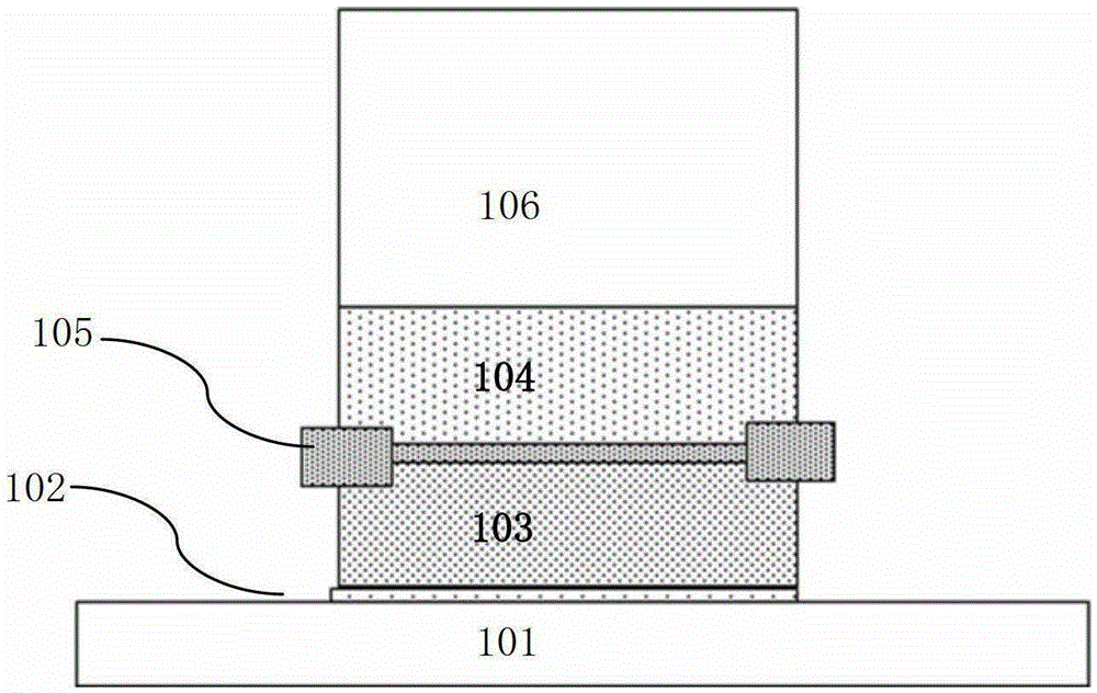
[0022] Step three, such as Figure 4B As shown, the second bo...
PUM
 Abstract
Description
Claims
Application Information