Large warp silicon wafer pre-alignment device and method

A pre-alignment and silicon wafer technology, which is applied in photolithographic process exposure devices, optics, instruments, etc., can solve the problem of increased vertical vibration at the edge of large warped silicon wafers, blurred images at the edge of silicon wafers, and inability to perform pre-alignment And other problems, to achieve the effect of clear image on the edge of the silicon wafer, high alignment accuracy, increased convenience and adaptability

Active Publication Date: 2014-03-26
SHANGHAI MICRO ELECTRONICS EQUIP (GRP) CO LTD
View PDF4 Cites 6 Cited by
  • Summary
  • Abstract
  • Description
  • Claims
  • Application Information

AI Technical Summary

Problems solved by technology

[0004] 1. The large warped silicon wafer exceeds the depth of field of the pre-alignment lens after loading, which makes pre-alignment impossible;
[0005] 2. The vertical vibration of the edge of the large warped silicon wafer increases during the rotation centering process, so that the edge image of the silicon wafer is blurred, the pre-alignment accuracy is reduced, and the pre-alignment process cannot even be completed
[0010] That is to say, the depth of field of the lens of the general machine vision pre-alignment system is too small (compared to the large-warped silicon wafer), and the implementation cost of increasing the depth of field is relatively high; there is no real-time compensation system in the process of silicon wafer pre-alignment. The amount of warping of the sheet is adjusted

Method used


Image

  • Large warp silicon wafer pre-alignment device and method
  • Large warp silicon wafer pre-alignment device and method
  • Large warp silicon wafer pre-alignment device and method

Examples


Embodiment Construction

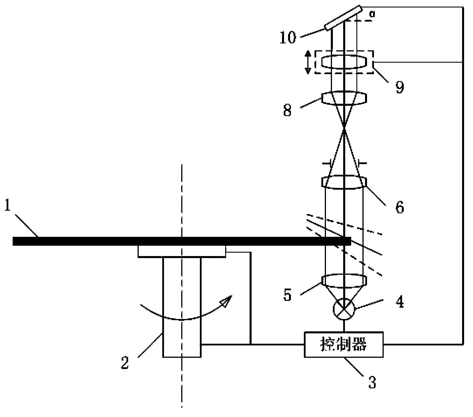
[0030] Below, the present invention will be further described in detail in conjunction with the accompanying drawings. This embodiment is implemented on the premise of the technical solution of the present invention, and detailed implementation methods and specific operating procedures are provided, but the protection scope of the present invention is not limited to the following the described embodiment.

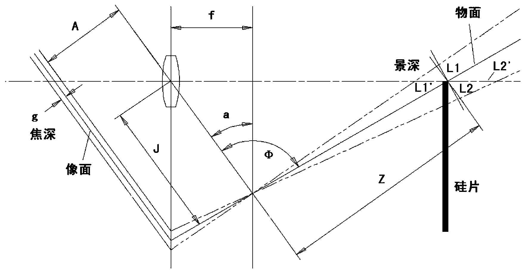
[0031] Due to the large deformation of the edge of the large warped silicon wafer, and when the size of the silicon wafer increases, the edge of the rotating silicon wafer vibrates greatly, which causes the image quality of the edge of the silicon wafer to deteriorate, and the pre-alignment accuracy decreases or cannot be completed. The invention provides a device and method for pre-alignment of silicon wafers used in photolithography machines, aiming to solve the problems of centering and orientation of large warped silicon wafers.

[0032] figure 1 It is a composition di...


PUM


Abstract

The invention provides a large warp silicon wafer pre-alignment device which is used for measuring the circle center and the direction of a silicon wafer. The pre-alignment device comprises a rotating platform which is used for absorbing the silicon wafer and driving the silicon wafer to rotate, a lighting source which is used for lighting edges of the silicon wafer, a pre-alignment imaging lens which is used for sampling images of the edges of the silicon wafer, adopts an object space telecentric lens or double telecentric lens, and comprises an imaging sensor, and a controller which is used for controlling the rotating platform, the lighting source and the pre-alignment imaging lens, and performing analysis and fitting on sampled images of the edges of the silicon wafer, so as to obtain the circle center and the direction of the silicon wafer, wherein the edges of the silicon wafer are imaged on the imaging sensor through the pre-alignment imaging lens after being lighted; and according to the proposal in the invention, the pre-alignment imaging lens also comprises an optimal object plane compensation system which is used for fixing an optimal object plane before sampling, and performing real-time compensation to object distances during sampling, so as to ensure that positions of all the edges of the silicon wafer can be clearly imaged.

Description

technical field [0001] The invention relates to the field of integrated circuit manufacturing, in particular to a pre-alignment device and method for large warped silicon wafers. Background technique [0002] Microelectronics technology plays an important role in the revolution of information industry, and photolithography machine is an indispensable tool in the manufacturing of microelectronic devices. In the production process of semiconductor devices, the silicon wafer needs to be transferred to the workpiece table with high centering and orientation accuracy through the silicon wafer transmission mechanism, so that the silicon wafer can be exposed in a fixed posture. Since the position and direction of the silicon wafer are uncertain when it is placed in the silicon wafer tank, it is required to pre-align the silicon wafer with a certain precision before the silicon wafer is transferred to the workpiece table, which is determined by measuring the center of the silicon wa...

Claims


Application Information

Patent Timeline
Patent Type & Authority Applications(China)
IPC IPC(8): H01L21/68G03F7/20G03F9/00
CPCG03F7/70G03F9/7011H01L21/681
Inventor 于大维潘炼东张冲
Owner SHANGHAI MICRO ELECTRONICS EQUIP (GRP) CO LTD
Why Eureka
Try Eureka