


Quick Research
Generate reliable direction feasibility study reports for your R&D in just a few steps.

Technical Q&A
Discover and master advanced knowledge NOW. Basics, ideas, possibilities, all at once.

Find Solutions
As an expert in R&D theories, this can generate solutions to your technical problems instantly.

Evaluate Feasibility
Analyze your overall solution with one click, know your potential R&D risks in advance.

Monitor Landscape
Get weekly tech updates, stay abreast of the latest tech innovations and key insights.
Structure to increase resistance to electromigration
A technology of electromigration and dielectric layer, applied in the field of resistance structure, can solve the problems of reducing metal diffusion rate and improving metal layer resistance
- Summary
- Abstract
- Description
- Claims
- Application Information
AI Technical Summary
Problems solved by technology
Method used
Image

Examples
Embodiment Construction
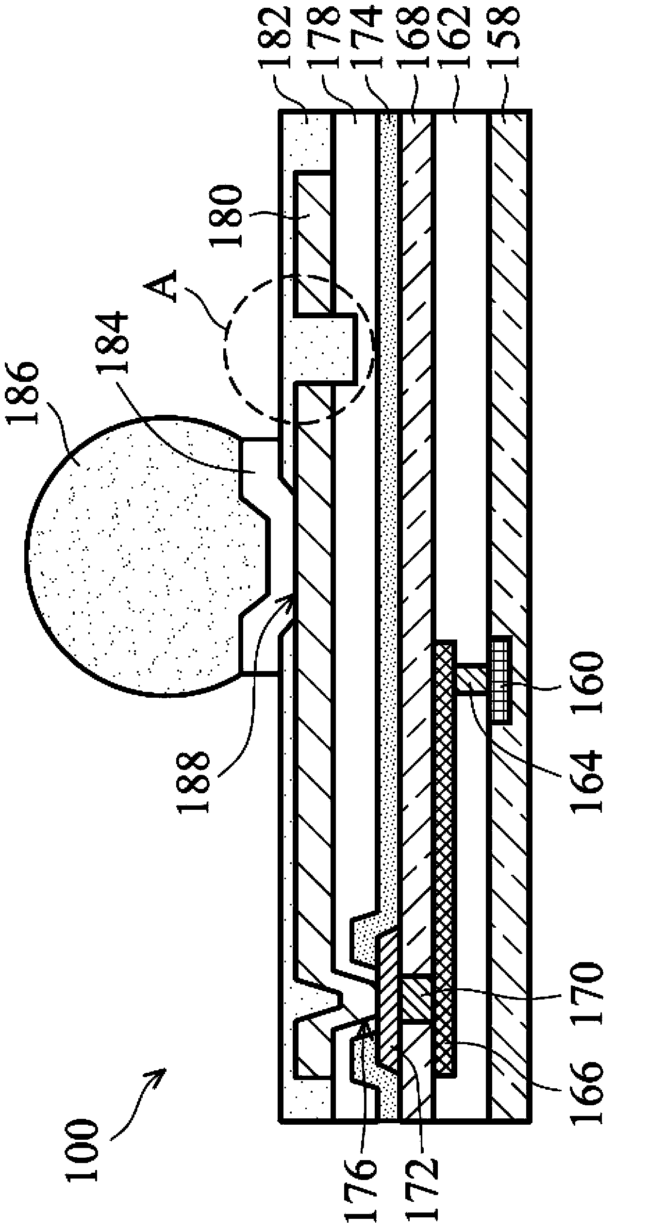
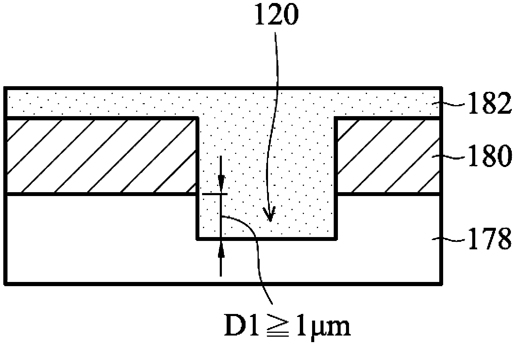
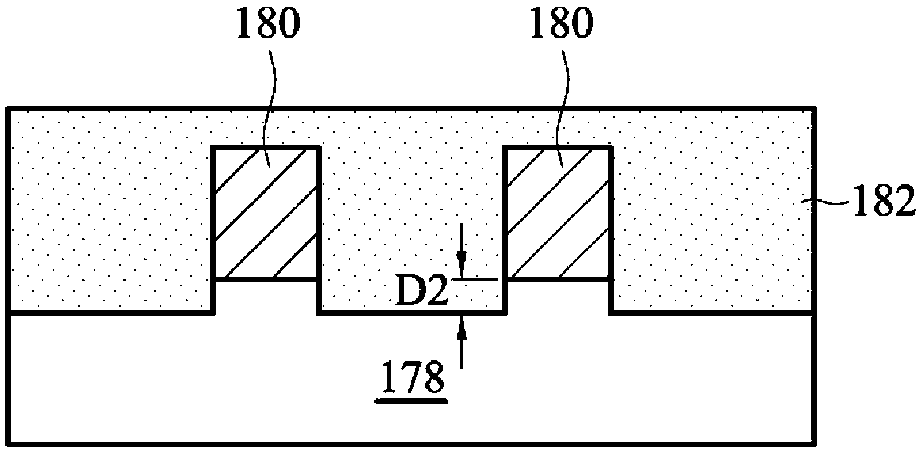
[0055] The making and using of some embodiments are discussed in detail below. It should be appreciated, however, that the present invention provides many applicable concepts that can be implemented in a wide variety of specific contexts. The specific embodiments discussed are merely illustrative of specific ways to make and use the invention, and do not limit the scope of the invention.
[0056] The invention is described below for an implementation in a specific context, using one or more solder balls, microbumps, metal pillars (eg, copper pillars), copper studs, gold studs, or combinations thereof. However, the present disclosure can also be applied to various packages in the semiconductor industry. It can be understood that the following disclosure provides many different implementations or examples for realizing different features. Specific examples of components or arrangements are described below to simplify the present disclosure. Of course, these are only examples ...
PUM
| Property | Measurement | Unit |
|---|---|---|
| Depth | aaaaa | aaaaa |
Abstract
Description
Claims
Application Information
 - R&D Engineer
- R&D Manager
- IP Professional
- Industry Leading Data Capabilities
- Powerful AI technology
- Patent DNA Extraction
Browse by: Latest US Patents, China's latest patents, Technical Efficacy Thesaurus, Application Domain, Technology Topic, Popular Technical Reports.
© 2024 PatSnap. All rights reserved.Legal|Privacy policy|Modern Slavery Act Transparency Statement|Sitemap|About US| Contact US: help@patsnap.com