Manufacturing method of field termination type insulated gate type bipolar transistor

A technology of bipolar transistor and insulated gate type, which is applied in the direction of transistor, semiconductor/solid-state device manufacturing, semiconductor device, etc., and can solve the problems of increasing manufacturing cost and high price of FS type IGBT process

Inactive Publication Date: 2014-04-02
CSMC TECH FAB2 CO LTD
View PDF2 Cites 2 Cited by
  • Summary
  • Abstract
  • Description
  • Claims
  • Application Information

AI Technical Summary

Problems solved by technology

[0004] Regardless of the above methods, expensive special equipment is required, which increases the manufacturing cost of the FS type IGBT

Method used


Image

  • Manufacturing method of field termination type insulated gate type bipolar transistor
  • Manufacturing method of field termination type insulated gate type bipolar transistor
  • Manufacturing method of field termination type insulated gate type bipolar transistor

Examples


Embodiment Construction

[0037] Introduced below are some of the various embodiments of the invention, intended to provide a basic understanding of the invention. It is not intended to identify key or critical elements of the invention or to delineate the scope of protection.

[0038] In order to make the object, technical solution and advantages of the present invention clearer, the present invention will be further described in detail below in conjunction with the accompanying drawings.

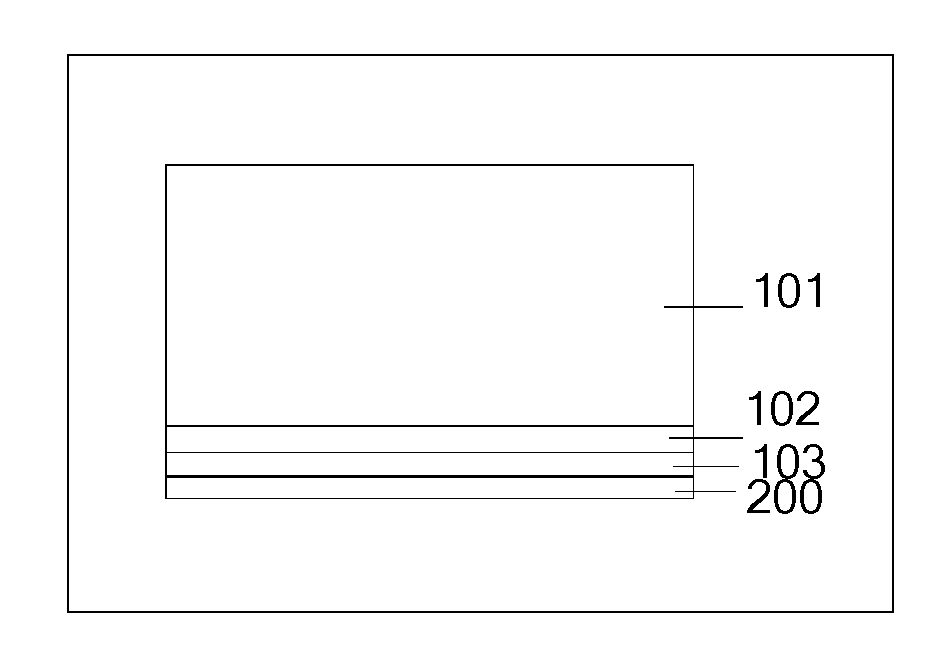
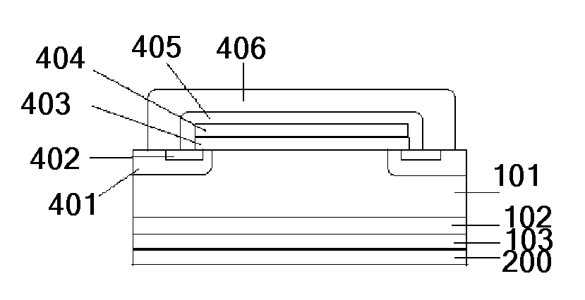
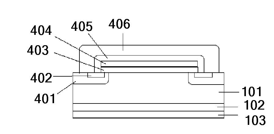
[0039] figure 1 , figure 2 , image 3 A schematic diagram showing the formation of the first substrate 100 in the manufacturing method of the field-stop type insulated gate bipolar transistor according to the embodiment of the present invention. Figure 4 It is a schematic diagram showing the formation of the stopper layer 200 in the manufacturing method of the field stop type insulated gate bipolar transistor according to the embodiment of the present invention. Figure 5 It is a schematic diagram showing the...


PUM


Abstract

The invention relates to a manufacturing method of a field termination type insulated gate type bipolar transistor. The method comprises the following steps in sequence: forming a first substrate, forming a termination layer on the back side of the first substrate, binding the first substrate with a second substrate of specified thickness through the termination layer in a direct binding mode, thinning the first substrate, forming a front side structure of IGBT (Insulated Gate Bipolar Translator) on the first substrate, removing the second substrate by taking the termination layer as the key point, and removing the termination layer. The method provided by the invention can be compatible with the conventional ordinary process, and is simple in process and high in efficiency, no special equipment is needed, and the process cost can be greatly lowered.

Description

technical field [0001] The present invention relates to the field of integrated circuit manufacturing, in particular to a method for manufacturing Field Stop (Field Stop, FS for short) insulated gate bipolar transistors (Insulated Gate Bipolar Transistor, IGBT for short) manufacturing by direct bonding. Background technique [0002] IGBT is a composite fully-controlled voltage-driven power semiconductor device composed of BJT (bipolar transistor) and MOS (insulated gate field effect transistor), which has both high input impedance of MOSFET and low conduction voltage drop of GTR. The advantages. The saturation voltage of GTR is low, the carrying current density is large, but the driving current is large; the driving power of MOSFET is small, the switching speed is fast, but the conduction voltage drop is large, and the current carrying density is small. The IGBT combines the advantages of the above two devices, with low driving power and low saturation voltage. [0003] Am...

Claims


Application Information

Patent Timeline
Patent Type & Authority Applications(China)
IPC IPC(8): H01L21/331
CPCH01L29/66333H01L29/7395H01L29/66325H01L21/6835
Inventor 黄璇王根毅邓小社
Owner CSMC TECH FAB2 CO LTD
Why Eureka
Try Eureka