Method for manufacturing conductive metal connecting piece connected with PCB and connecting piece
A metal conductive, PCB board technology, applied in the direction of connection, fixed connection, contact parts, etc., can solve the problems of the bonding stability of the conductive connector and the PCB board, poor comprehensive performance of the formability, etc., and achieve high physical metallurgical bonding strength. , Reduce the cost of the process, the effect of good workability
- Summary
- Abstract
- Description
- Claims
- Application Information
AI Technical Summary
Problems solved by technology
Method used
Image

Examples
Embodiment 1
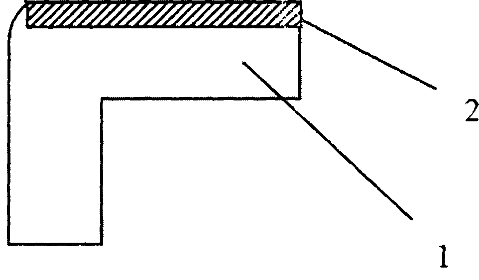
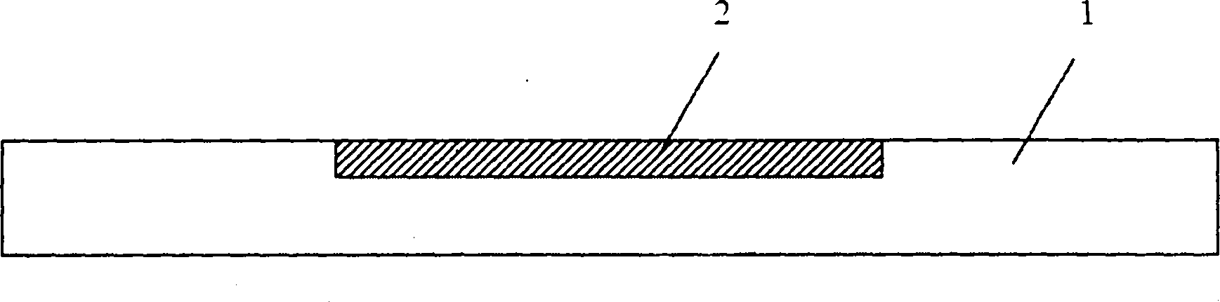
[0051] This embodiment provides a method for preparing a metal conductive connector connected to a PCB board. The raw materials used in the method: include a nickel base material of 30mm (width)*1.5mm (thickness), 0.15mm (thickness)*8mm (wide) pure copper tape.
[0052] The method comprises the steps of:
[0053] Step (1): On the surface of the pure nickel strip 1, a groove with a rectangular cross-section is continuously planed, the groove width is 8.1mm, and the depth is 0.15mm, and a pure copper strip is embedded in the groove of the pure nickel base material as The mosaic layer is formed into a composite metal strip with a thickness of 0.6mm through cold compound rolling with a rolling deformation rate of 60% at the corresponding fitting position. Wherein, the width of the mosaic layer-copper strip before rolling and compounding is 98.77% of the total width of the groove;
[0054] Step (2): Carry out three times of softening annealing process to the clad metal strip afte...
Embodiment 2
[0062] This embodiment provides a method for preparing a metal conductive connector connected to a PCB board. The raw material is a nickel base material of 30mm (width)*1.5mm (thickness), copper of 0.3mm (thickness)*8mm (width). -Silver layered composite material, in which the silver layer accounts for 10% of the total thickness of the copper-silver layered composite material, and the copper layer accounts for 90%. The copper-silver layered composite material is compounded by the existing preparation technology.
[0063] The method comprises the steps of:
[0064] Step (1): On the surface of the pure nickel strip, continuously plan a groove with a rectangular cross-section, the groove width is 8.2mm, and the depth is 0.3mm, and the copper-silver layer is embedded in the groove of the pure nickel substrate. The composite material is used as an inlay layer, and a composite metal strip with a thickness of 0.6mm is obtained through cold composite rolling with a rolling deformation...
Embodiment 3
[0070] This embodiment is an improvement on the basis of Embodiment 1, and provides a method for bending a metal conductive connector. The method includes steps 1-3 of the preparation method described in Example 1, and further includes step (4): bending and forming the conductive connector obtained in step (3).
[0071] According to the characteristics of inlaid copper that are easy to oxidize and discolor, generally the conductive connectors after stamping should be treated and protected to facilitate the subsequent brazing process.
[0072] After the SMT process, the outer surface of the inlay layer 2 is connected to the PCB board 3 through soldering. After mass testing, the anti-peeling pull-out force between the metal conductive connector and the PCB board 3 is above 1.6kgf, far exceeding the standard application requirement of 1.2kgf.
PUM
| Property | Measurement | Unit |
|---|---|---|
| Thickness | aaaaa | aaaaa |
| Size | aaaaa | aaaaa |
| Groove width | aaaaa | aaaaa |
Abstract
Description
Claims
Application Information
 - R&D Engineer
- R&D Manager
- IP Professional
- Industry Leading Data Capabilities
- Powerful AI technology
- Patent DNA Extraction
Browse by: Latest US Patents, China's latest patents, Technical Efficacy Thesaurus, Application Domain, Technology Topic.
© 2024 PatSnap. All rights reserved.Legal|Privacy policy|Modern Slavery Act Transparency Statement|Sitemap