Photoelectric functional structure unit and production method and application thereof
A structural unit and multi-functional technology, applied in the direction of electrical components, etc., can solve the problems of approaching the physical limit of micro-machining technology, low recording density, slow reading and writing speed, etc.
- Summary
- Abstract
- Description
- Claims
- Application Information
AI Technical Summary
Problems solved by technology
Method used
Image
Examples
Embodiment 1
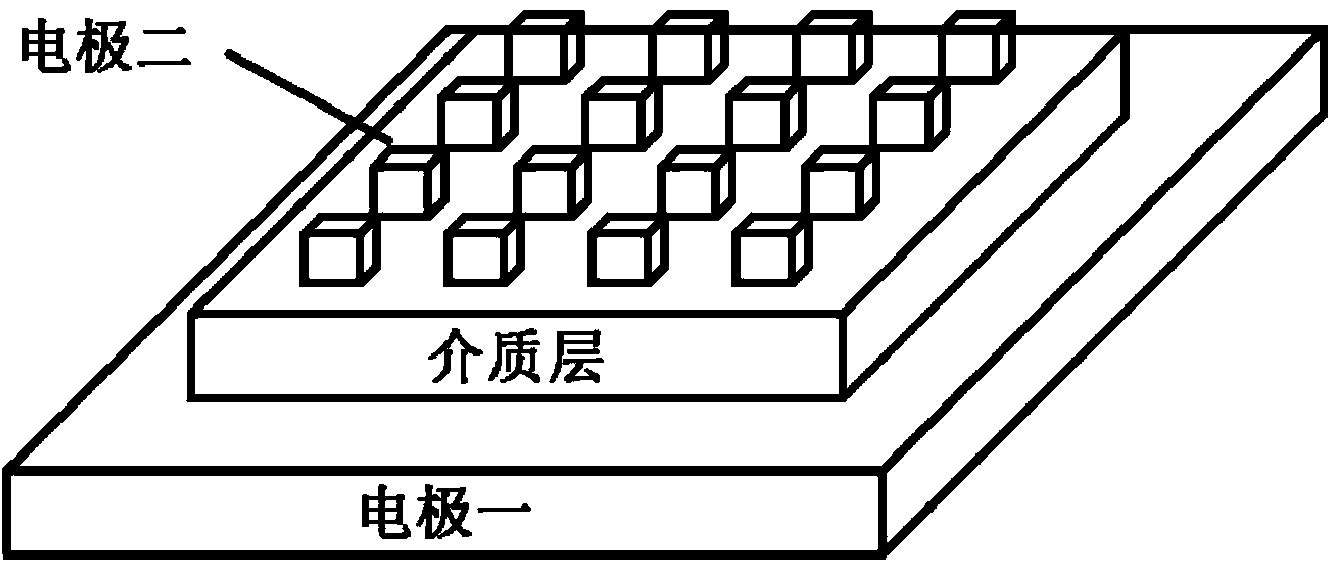
[0027] In this embodiment, the structure of the photoelectric multifunctional structural unit is as follows figure 1 As shown, it consists of electrode one, electrode two, and a dielectric layer between electrode one and electrode two. The first electrode uses a heavily doped Si substrate, the dielectric layer uses a cerium oxide film with a thickness of 80nm, and the second electrode uses an ITO electrode.
[0028] The photoelectric multifunctional structural unit mentioned above is prepared by coating method, as follows:
[0029] Step 1: Ultrasonic clean the heavily doped Si substrate with acetone for 10 minutes, then ultrasonically clean it with ethanol for 10 minutes after taking it out, and then ultrasonically clean it with deionized water for 10 minutes to remove surface impurities; then blow it with nitrogen Dry, soak in 10% HF solution for 120 seconds to remove the oxide layer on the surface, ultrasonically clean with acetone for 10 minutes after taking out, ultrasoni...
PUM
 Abstract
Description
Claims
Application Information
 - R&D
- Intellectual Property
- Life Sciences
- Materials
- Tech Scout
- Unparalleled Data Quality
- Higher Quality Content
- 60% Fewer Hallucinations
Browse by: Latest US Patents, China's latest patents, Technical Efficacy Thesaurus, Application Domain, Technology Topic, Popular Technical Reports.
© 2025 PatSnap. All rights reserved.Legal|Privacy policy|Modern Slavery Act Transparency Statement|Sitemap|About US| Contact US: help@patsnap.com


