Packaging structure applied to long-pulse-width and high-power semiconductor laser

A packaging structure and laser technology, applied in the laser field, can solve problems such as heat dissipation differences, and achieve the effects of alleviating stress and strain differences, improving heat dissipation efficiency, and reducing temperature differences

Inactive Publication Date: 2014-04-23
SUZHOU INST OF BIOMEDICAL ENG & TECH CHINESE ACADEMY OF SCI
View PDF9 Cites 20 Cited by
  • Summary
  • Abstract
  • Description
  • Claims
  • Application Information

AI Technical Summary

Problems solved by technology

[0013] The purpose of the present invention is to overcome the above problems in the prior art, provide a hard solder packaging structure, effectively solve and avoid the problem of heat dissipation difference between the n-plane and p-plane caused by lon

Method used


Image

  • Packaging structure applied to long-pulse-width and high-power semiconductor laser
  • Packaging structure applied to long-pulse-width and high-power semiconductor laser
  • Packaging structure applied to long-pulse-width and high-power semiconductor laser

Examples


Embodiment Construction

[0031] The present invention will be described in detail below with reference to the accompanying drawings and in combination with embodiments.

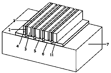
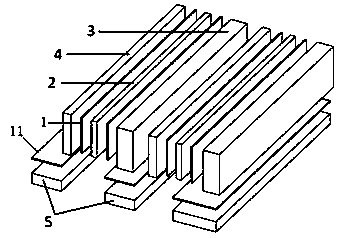
[0032] like figure 1 As shown, a high-power semiconductor laser packaging structure applied to long pulse width, including high-temperature hard solder 1, hard solder 11, semiconductor laser bar 2, p-plane sub-heat sink 3, n-plane sub-heat sink 4, electrical insulation Heat sink 5, soft solder 6 and heat sink 7, such as figure 2 As shown, the large surfaces of the n-plane sub-heat sink 4, the semiconductor laser bar 2 and the p-plane sub-heat sink 3 are stacked in sequence, and then the high-temperature hard solder 1 is used for high-temperature reflow soldering between each stacked surface. It is formed into a bar stack unit, and the electrical insulation heat dissipation is stacked on the long side of the same side of the n-plane sub-heat sink 4 and the p-plane sub-heat sink 3 in the above-mentioned welded bar stack unit. sheet ...


PUM

PropertyMeasurementUnit
Gap widthaaaaaaaaaa

Abstract

The invention discloses a packaging structure applied to a long-pulse-width and high-power semiconductor laser. The packaging structure comprises a high-temperature hard solder, a semiconductor laser bar, a p-surface secondary heat sink, an n-surface secondary heat sink, an electric insulation cooling fin, a soft solder and a heat sink, wherein the p-surface secondary heat sink, the n-surface secondary heat sink, the semiconductor laser bar, the high-temperature hard solder piece and the electric insulation cooling fin are stacked according to a certain structure and a certain sequence to form a laser bar stack through one-time or multi-time high-temperature backflow molding; the stack and the heat sink are subjected to backflow welding molding through the soft solder with relatively low temperature. According to the technical scheme, the temperature difference between a p surface and an n surface is small under the working condition of laser, the cooling efficiency is high, the stress-strain difference caused by the temperature difference is effectively reduced, and on the premise that the service life, conversion efficiency and other photoelectric performances of a device are not affected, the device of the structure can be used under the condition that the current duty ratio reaches 40 percent, namely the pulse width is 1-400mS.

Description

technical field [0001] The invention belongs to the technical field of lasers, and in particular relates to a packaging structure of a high-power semiconductor laser applied to a long pulse width. Background technique [0002] In 1960, Maiman manufactured the first ruby ​​laser, which opened the prelude to laser medicine. In 1961, the ruby ​​laser was first applied to the treatment of ophthalmic diseases, creating a precedent for the application of laser in medicine. With the development of laser medicine and The application of laser in various fields continues to deepen, and can be widely used in the diagnosis and treatment of various diseases such as internal medicine, surgery, women, children, eyes, ENT, skin, and plastic surgery. With the expansion of the wavelength range of semiconductor lasers, semiconductor lasers have been used in soft tissue resection, tissue bonding, coagulation, and vaporization, and have been widely used in medicine, as shown in Table 1. Semicon...

Claims


Application Information

Patent Timeline
IPC IPC(8): H01S5/00H01S5/022H01S5/02H01S5/024
Inventor 张丽芳江先锋李江
Owner SUZHOU INST OF BIOMEDICAL ENG & TECH CHINESE ACADEMY OF SCI
Why Eureka
Try Eureka