A kind of growth method of gan nanowire

A growth method and nanowire technology, which is applied to the growth of GaN nanowires and the field of growing GaN nanowires, can solve the problems of high price, difficulty in preparing large-size sapphire substrates, and high price, and achieve the effect of avoiding contamination

Inactive Publication Date: 2016-07-13
SOUTH CHINA NORMAL UNIVERSITY
View PDF9 Cites 0 Cited by
  • Summary
  • Abstract
  • Description
  • Claims
  • Application Information

AI Technical Summary

Problems solved by technology

For sapphire, its price is more expensive, and it is also difficult to prepare large-sized sapphire substrates
On the other hand, silicon substrates are cheaper and have a mature preparation process, so large-sized silicon substrates can be produced. However, when GaN is grown on a silicon substrate, it is easy to form remelting between Ga and silicon atoms on the surface of the substrate, and the crystal lattice and thermal expansion rate Large mismatch requires complex buffer layer design
For silicon carbide, it is too expensive and not suitable for large-scale applications

Method used


Image

  • A kind of growth method of gan nanowire
  • A kind of growth method of gan nanowire
  • A kind of growth method of gan nanowire

Examples


Embodiment 1

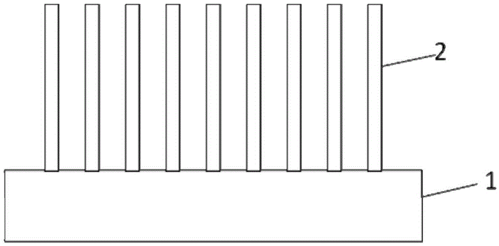
[0037] Sample pattern diagram of GaN nanowires grown on quartz substrate figure 2 As shown, from bottom to top are, quartz substrate, GaN nanowire; its preparation method is:

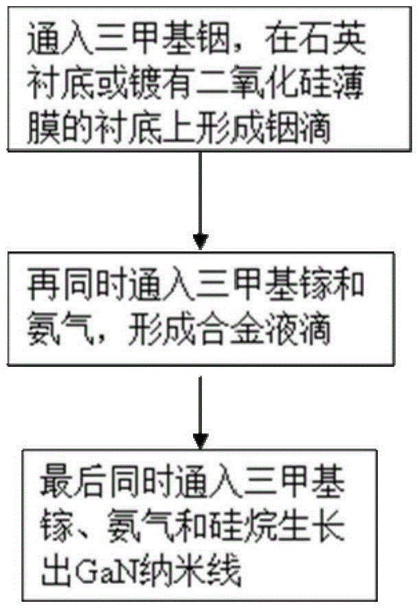
[0038] 1) Put the quartz substrate into the MOCVD reaction chamber, and heat-treat the substrate at 1000°C for 15 minutes in a hydrogen atmosphere;

[0039] 2) At 700°C, with a bias voltage of 400mbar, trimethylindium (TMIn) was injected for 30s, and liquid indium droplets were formed on the substrate with a density of about 8×10 6 piece / cm 2 ;

[0040] 3) Then feed ammonia gas and trimethylgallium (TMGa) at the same time, the molar flow rate of trimethylgallium is 60 μmol / min, the molar flow rate of ammonia gas is 50 times that of trimethylgallium, and GaN is formed and dissolved in indium droplets , forming alloy droplets with a droplet diameter of 100-300nm;

[0041] 4) Finally, ammonia gas, trimethylgallium (TMGa) and silane are introduced at the same time. The flow rate of ammonia gas and trim...

Embodiment 2

[0043] Sample pattern diagram of GaN nanowires grown on quartz substrate figure 2 As shown, from bottom to top are, quartz substrate, GaN nanowire; its preparation method is:

[0044] 1) Put the quartz substrate into the MOCVD reaction chamber, and heat-treat the substrate at 1000°C for 20 minutes in a hydrogen atmosphere;

[0045] 2) At 600°C, with a bias voltage of 350mbar, trimethylindium (TMIn) was pre-introduced for 150s to form liquid-phase indium droplets on the substrate with a density of about 6×10 7 piece / cm 2 ;

[0046] 3) Then feed ammonia gas and trimethylgallium (TMGa) at the same time, the molar flow rate of trimethylgallium is 60 μmol / min, and the molar flow rate of ammonia gas is 100 times that of trimethylgallium, so that GaN is formed and dissolved in indium drops, forming alloy droplets with a diameter of 100-300nm;

[0047] 4) Finally, ammonia gas, trimethylgallium (TMGa) and silane are introduced at the same time. The flow rate of ammonia gas and tri...

Embodiment 3

[0049] Sample pattern diagram of GaN nanowires grown on quartz substrate figure 2 As shown, from bottom to top are quartz substrate and GaN nanowire. Its preparation method is:

[0050]1) Put the quartz substrate into the MOCVD reaction chamber, and heat-treat the substrate at 1100°C for 20 minutes in a hydrogen atmosphere;

[0051] 2) At 600°C, with a bias voltage of 450mbar, trimethylindium (TMIn) was introduced for 300s to form liquid indium droplets on the substrate with a density of about 5×10 8 piece / cm 2 ;

[0052] 3) Then feed ammonia gas and trimethylgallium (TMGa) at the same time, the molar flow rate of trimethylgallium is 80 μmol / min, and the molar flow rate of ammonia gas is 10 times that of trimethylgallium, so that GaN is formed and dissolved in indium drops, forming alloy droplets with a diameter of 400-500nm;

[0053] 4) Finally, ammonia gas, trimethylgallium (TMGa) and silane are introduced at the same time. The flow rate of ammonia gas and trimethylgal...


PUM

PropertyMeasurementUnit
lengthaaaaaaaaaa
diameteraaaaaaaaaa
heightaaaaaaaaaa

Abstract

The invention discloses a method for growing GaN nanowires. The steps of the method include: pre-introducing trimethyl indium on a quartz substrate or a substrate coated with a layer of silicon dioxide film on the surface, so that a liquid is formed on the surface of the substrate. Phase indium drop, and then feed trimethylgallium and ammonia gas at the same time to form alloy droplets; finally feed trimethylgallium, ammonia gas and silane at the same time to grow GaN nanowires on the alloy droplets. The method of the present invention uses trimethyl indium as the source of indium catalyst, and realizes the controllable growth of high-quality GaN nanowires on cheap and easy-to-obtain quartz or a substrate coated with a silicon dioxide film on the surface; and belongs to in-situ introduction , without the cumbersome process of transferring and cleaning between different devices, effectively avoiding the contamination of samples during the transfer process; and without the need for complicated buffer layer design, the operation is simple and easy, which is conducive to industrial production.

Description

technical field [0001] The invention belongs to the technical field of semiconductor material growth, and relates to a method for growing GaN nanowires, in particular to a method for growing GaN nanowires on a quartz substrate or a substrate coated with a silicon dioxide film. Background technique [0002] GaN-based semiconductor materials have a wide direct bandgap, and are widely used in high-frequency, high-temperature, high-power electronic devices and Optoelectronic devices and other fields have become the third generation of semiconductor materials after the first generation of germanium (Ge), silicon (Si) semiconductor materials and the second generation of gallium arsenide (GaAs), indium phosphide (InP) compound semiconductor materials. [0003] MOCVD (Metal Organic Compound Chemical Vapor Deposition) and MBE (Molecular Beam Epitaxy) are two main techniques for growing high-quality semiconductor materials, which are unmatched by other techniques. Especially MOCVD te...

Claims


Application Information

Patent Timeline
Patent Type & Authority Patents(China)
IPC IPC(8): C30B25/02C30B25/18C30B29/38C30B29/62C01B21/06
Inventor 李述体刁家声王幸福
Owner SOUTH CHINA NORMAL UNIVERSITY
Why Eureka
Try Eureka