Unlock instant, AI-driven research and patent intelligence for your innovation.

A tsv hole filling method

A technology of hole wall and silicon micro-hole, which is applied in the field of three-dimensional packaging of microelectronics, and can solve problems such as application limitations of electrical performance of chips

Active Publication Date: 2016-07-06
NAT CENT FOR ADVANCED PACKAGING CO LTD
View PDF5 Cites 0 Cited by
  • Summary
  • Abstract
  • Description
  • Claims
  • Application Information

AI Technical Summary

Problems solved by technology

[0003] The purpose of the embodiment of the present invention is to provide a TSV hole filling method to solve the limitation of the chip electrical performance application caused by the difference in the thickness of the insulating layer in the microhole

Method used


Image

  • A tsv hole filling method
  • A tsv hole filling method
  • A tsv hole filling method

Examples


Embodiment Construction

[0028] In order to better understand the above technical solutions, the above technical solutions will be described in detail below with reference to the accompanying drawings and specific embodiments.

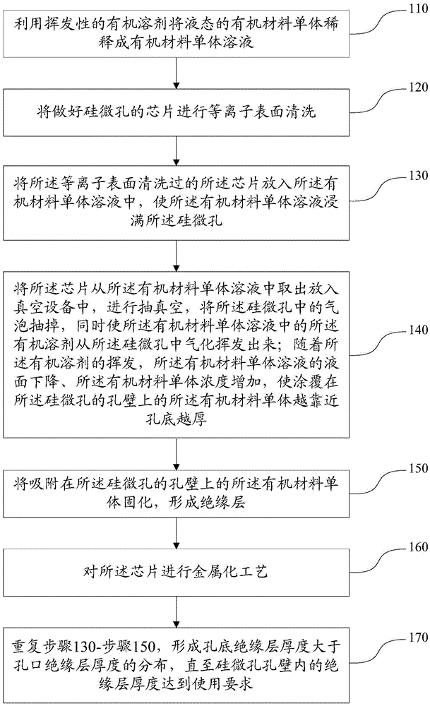
[0029] like figure 1 As shown, an embodiment of the present invention provides a TSV hole filling method, including the following steps:

[0030] Step 110: diluting the liquid organic material monomer into an organic material monomer solution with a volatile organic solvent;

[0031] Specifically, the organic material monomer is diluted with the organic solvent to 0.1%-20%, so that the organic material monomer solution has very low surface tension. The organic material monomer in this embodiment is a high temperature resistant insulating resin material after curing, and polyimide or benzocyclobutene is the first choice. These two materials have the characteristics of high temperature resistance, low dielectric constant and low high frequency loss. It is suitable for the tran...


PUM


Abstract

The invention discloses a TSV hole filling method, comprising the following steps: using a volatile organic solvent to dilute a liquid organic material monomer into an organic material monomer solution; performing plasma surface cleaning on a chip with silicon micropores; The chip cleaned by the plasma surface is put into the organic material monomer solution, so that the organic material monomer solution is filled with silicon micropores; the chip is taken out from the organic material monomer solution and placed in a vacuum device, and the silicon micropore is vacuumized. The bubbles in the pores are pumped out, and the organic solvent is vaporized and volatilized from the silicon micropores; the organic material monomer adsorbed on the pore wall of the silicon micropores is solidified to form an insulating layer; the chip is metallized. The present invention forms in the silicon micropore through the above steps an insulating layer whose thickness gradually increases from the opening to the bottom of the hole. When the insulating layer at the opening of the silicon micropore meets the electronic performance requirements, the insulating layer in the silicon micropore must meet Electrical performance requirements.

Description

technical field [0001] The invention relates to the technical field of microelectronic three-dimensional packaging, in particular to a TSV hole filling method. Background technique [0002] TSV technology in 3D packaging is the key content of current research and development. TSV hole filling requires micron-level high aspect ratio microholes to be processed on the silicon surface. In the high aspect ratio microholes, an insulating layer is first made, and then a metal barrier layer is made. The seed layer is electroplated and the holes are then filled by electroplating. In the TSV hole filling process, it is very difficult to fabricate the insulating layer. Now the main technology is PVD deposition, PECVD deposition of silicon oxide or silicon nitride technology. Due to the high aspect ratio of silicon micropores, the orifice is only a few microns in diameter and deep The aspect ratio is usually greater than 5:1, so neither the PVD method nor the PECVD equipment using TEOS...

Claims


Application Information

Patent Timeline
Patent Type & Authority Patents(China)
IPC IPC(8): H01L21/768
CPCH01L21/76898
Inventor 于中尧
Owner NAT CENT FOR ADVANCED PACKAGING CO LTD