Large image plane high resolution optical lens

A high-resolution, optical lens technology, applied in optics, optical components, installation, etc., can solve problems such as vignetting, failure to reach large chips, and high price, and achieve the effect of good process performance and low material cost

Inactive Publication Date: 2014-05-07
SUZHOU LIGHTLNS OPTICAL TECH
View PDF0 Cites 4 Cited by
  • Summary
  • Abstract
  • Description
  • Claims
  • Application Information

AI Technical Summary

Problems solved by technology

However, if the designed imaging surface of the optical lens does not reach the size of the large chip, it will cause a certain degree of vignetting
The current optical lens with a focal length of f = 25mm on the market generally has an imaging surface of 2 / 3″ and 3 / 4″, and there are few products that can reach 1 / 1″, and the price is relatively expensive

Method used


Image

  • Large image plane high resolution optical lens
  • Large image plane high resolution optical lens
  • Large image plane high resolution optical lens

Examples


Embodiment Construction

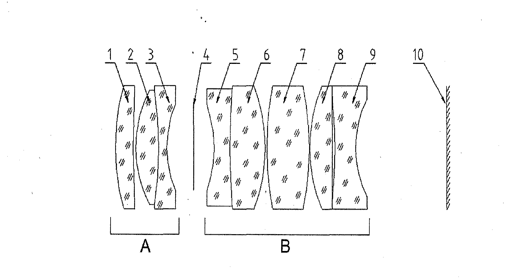
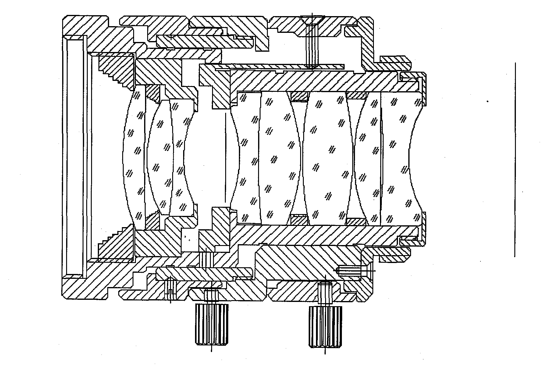
[0026] 1. If figure 1 As shown, a large image surface high-resolution optical lens described in this patent, from left to right is: concave-convex lens 1, biconvex lens 2, biconcave lens 3, biconcave lens 5, biconvex lens Lens 6', biconvex lens 7, plano-convex lens 8 and biconcave lens 9.

[0027] 2. If figure 2 As shown, a large image surface high-resolution optical lens described in this patent is characterized in that a gasket is arranged between the cemented lens composed of the concave-convex lens 1, the biconvex lens 2 and the biconcave lens 3, Make the center interval between the two be 0.34mm, another gasket is provided between the cemented lens composed of biconcave lens 5 and biconvex lens 6 and biconvex lens 7, so that the center interval between the two is 1.52mm A gasket is also provided between the biconvex lens 7 and the plano-convex lens 8, so that the center interval between the two is 0.25mm, and the plane contact between the plano-convex lens 8 and the bi...


PUM


Abstract

The invention relates to a large image plane high resolution optical lens and belongs to the field of optical-mechanical-electronic integration. An optical system comprises 8 lenses, an aperture 4 and an imaging surface 10. A model is formed through the optimization and evolution of a double Gauss structure, through the reasonable allocation of optical power, the pixel can reach 8 million pixels, an image plane can reach 1 / 1'', and the structure is compact. According to the optical lens, a spherical design is employed, the processing performance is good, and the material cost is low. The product can be widely applied to the fields of industrial measurement and detection, intelligent transportation and the like.

Description

technical field [0001] The invention relates to an optical imaging system, in particular to an optical lens with high resolution and large image surface. It can be widely used in opto-mechanical-electrical integration fields such as intelligent transportation, industrial detection, and optical imaging. Background technique [0002] With the continuous development of modern optical technology, in the fields of industrial inspection and intelligent transportation, the chip size of optical imaging is getting bigger and bigger. Common large-size CCD / CMOS are 1 / 1.8″, 2 / 3″, 3 / 4″, etc. In recent years, 1 / 1″ and 4 / 3″ have appeared on the market. But if the designed imaging surface of the optical lens does not reach the size of a large chip, it will cause a certain degree of vignetting. Currently Optical lenses with a focal length of f=25mm on the market generally have an imaging surface of 2 / 3″ and 3 / 4″, and there are few products that can reach 1 / 1″, and the price is relatively e...

Claims


Application Information

Patent Timeline
Patent Type & Authority Applications(China)
IPC IPC(8): G02B13/00G02B7/02
Inventor 吴连平连建英陈艺敏
Owner SUZHOU LIGHTLNS OPTICAL TECH
Why Eureka
Try Eureka