

Electronic component
一种电子部件、构件的技术,应用在混合电容器端子、电解电容器、混合/双电层电容器制造等方向,能够解决耐压下降、出现裂缝、壳体2熔化等问题,达到抑制润湿扩展的效果
Active Publication Date: 2014-05-07
MURATA MFG CO LTD
View PDF5 Cites 0 Cited by
- Summary
- Abstract
- Description
- Claims
- Application Information
AI Technical Summary
Problems solved by technology
In addition, when the melted high-temperature solder 7 comes into contact with the case 2 made of resin, a part of the case 2 will melt or cracks 8 will occur.
[0004] For example, in the case of an electronic component such as an electric double layer capacitor using an organic electrolytic solution, the capacitor element and the organic electrolytic solution are housed in the case 2, and the intrusion of moisture from the outside is strictly prohibited. The problem
Method used
View moreImage
Smart ImageViewing Examples

Examples
Embodiment
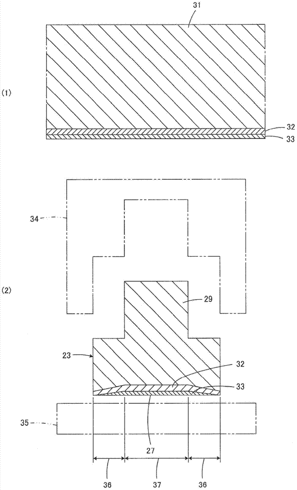
[0062] As a plate, an aluminum plate with a thickness of 0.5 mm was prepared, and after zincate treatment (zincate treatment) was implemented on one of its main surfaces, a matte nickel plated film with a thickness of 0.66 μm was formed as a base plated film, and a thickness of 0.66 μm was formed on it. 0.15μm gold plating film, as the outer layer plating film. Afterwards, by implementing the reference image 3 The described press forming and the like can obtain the external terminal member according to the examples.
Login to View More PUM
 Abstract
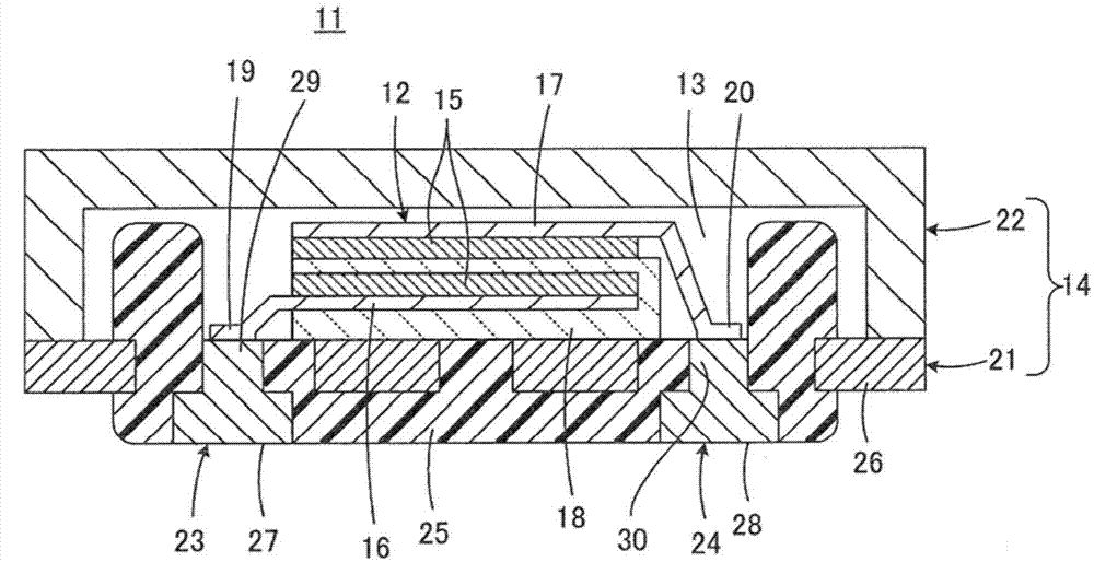
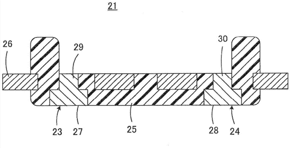
In an electronic component including an external terminal member and an insulating section contacting with the external terminal member while taking a specified surface side of the external terminal member as an exposed portion, when melted solder is applied onto the external terminal member, a part of the insulating section may melt or a crack may enter the insulating part sometimes. The exposed part (27) of the external terminal member (23) of the invention is provided by a base plating film (32) and an outer plating film (33), wherein the base plating film is made of nickel or a nickel alloy and the outer plating film which is placed on the base plating film and is made of gold, tin, or an alloy containing at least one of gold and tin. The outer plating film (33) is formed in a mode that a relatively thin region (36) surrounding a relatively thick region (37). The amount of metal having good solder wettability in the relatively thin region is small (36) and the base plating film is likely to be oxidized. Therefore, the periphery of the exposed portion (27) of the external terminal member (23) is reduced in solder wettability so that the spread of the solder can be suppressed.
Description
technical field [0001] The present invention relates to an electronic component, and particularly to an electronic component that includes an electrically insulating insulating portion and an external terminal member embedded in the insulating portion, and is mounted with solder applied to the external terminal member. Background technique [0002] As a technique related to the present invention, it is described in, for example, JP-A-2011-100998 (Patent Document 1). Especially in Patent Document 1 figure 1 as well as image 3 describes a case of an electric double layer capacitor composed of a concave main body and a lid. The case is made of resin, and the external terminal member is embedded in the case. Figure 5 In FIG. 2 , the above-mentioned structure is generalized, and a state in which the external terminal member 1 is fitted into the case 2 serving as an insulating portion is shown in a cross-sectional view. [0003] Such as Figure 5 As shown, when the electron...
Claims
Login to View More Application Information
Patent Timeline
 Patent Type & AuthorityApplications(China)
IPC IPC(8): H01G11/74H01G11/82H01G11/80H01G11/84
CPCH01G11/74H01G11/80H01G11/82Y02E60/13
Inventor原田裕之板谷昌治
OwnerMURATA MFG CO LTD