Electronic Devices and Methods of Making Them Using Solution Processing Techniques

a technology of electroelectronic devices and processing techniques, applied in the direction of electroluminescent light sources, thermoelectric devices, electric lighting sources, etc., can solve the problems of increasing manufacturing time and complexity, increasing cost, and process not removing inorganic materials of the underlying layer, so as to improve increase the wettability of the surface, and reduce the wettability of the second layer of bank material

Inactive Publication Date: 2011-05-05
CAMBRIDGE DISPLAY TECH LTD
View PDF22 Cites 25 Cited by
  • Summary
  • Abstract
  • Description
  • Claims
  • Application Information

AI Technical Summary

Benefits of technology

[0067]The present applicant has yet further found that baking can decrease the wettability of the second layer of bank material. As such, they have found it beneficial to provide a baking step prior to deposition of organic material from solution. The bake may be at a temperature in the range 150 to 250° C., more preferably, 170 to 210° C., most preferably 180 to 200° C. The bake is preferably performed in an inert atmosphere such as N2. For an organic light-emissive device, hole injecting material such as PEDOT may be deposited prior to the bake such that the hole injecting layer and the bank structure are baked at the same time prior to deposition of the organic light-emissive material in the wells.
[0068]Yet another problem that the present applicant has identified is that after forming the wells in a bank structure, it is desirable to provide a cleaning step such as an O2 plasma treatment. Such a step cleans the surfaces in the wells and increases wettability of these surfaces prior to deposition or organic material therein. However, the present applicant has found that such a step greatly increases the wettability of surfaces of the bank which have been previously treated with, for example, a fluorine based plasma treatment in order to decrease their wettability. In fact, contact angles of such a treated surface can drop to under 10° after such a cleaning step. As such, when containment of organic material in the wells has been an issue, such a cleaning step had to be avoided. In contrast, the present applicant has found that when using a double bank structure with an inherently low wetting second layer, the cleaning step can be performed while retaining good de-wetting characteristics over the bank. For example, the contact angle for Cytop-type materials remains over 100° even after an O2 plasma cleaning step.

Problems solved by technology

The present applicant has realized that while double bank step structures can be advantageous for containment of organic material deposited from solution, the multiple steps required to form such structures can increase manufacturing time and complexity thus increasing cost.
This process does not remove the inorganic material of the underlying layer.

Method used


Image

  • Electronic Devices and Methods of Making Them Using Solution Processing Techniques
  • Electronic Devices and Methods of Making Them Using Solution Processing Techniques
  • Electronic Devices and Methods of Making Them Using Solution Processing Techniques

Examples


Embodiment Construction

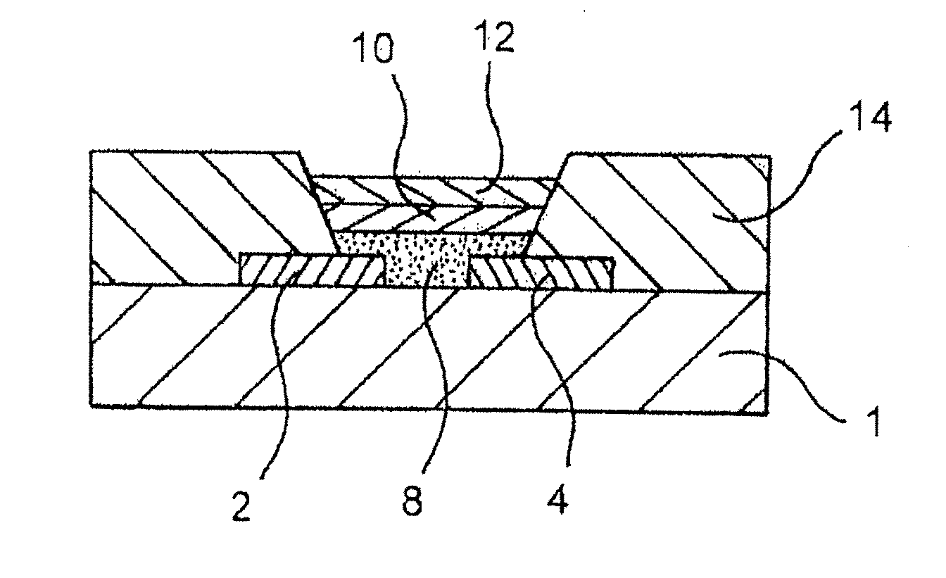
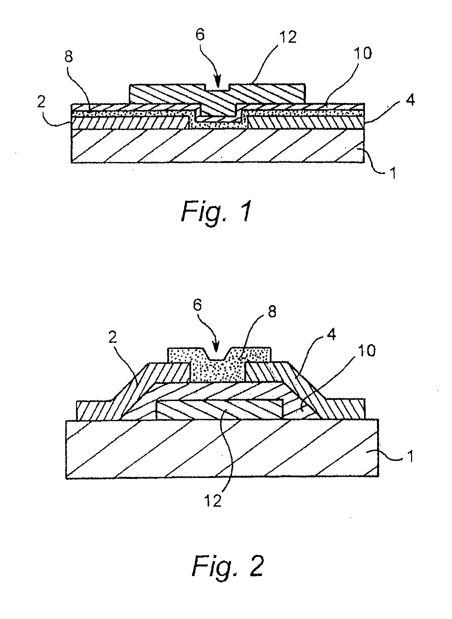
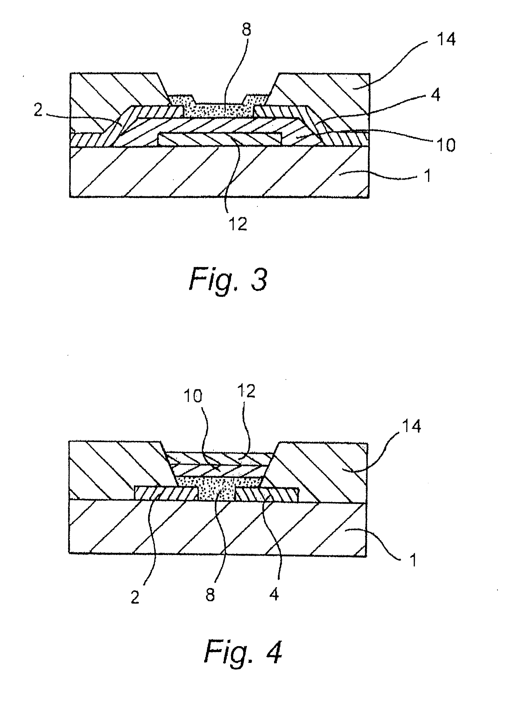
[0091]Embodiments of the present invention relate to printed electronic devices which comprise a patterned well-defining bank structure and methods of making the same. A double bank well-defining structure is formed by removing material from first and second bank layers in a single processing step whereby a step structure is formed due to a difference in removal rate of the material of the first and second layers.

[0092]FIG. 7 shows a double bank structure according to an embodiment of the present invention. The double bank structure is disposed on an electronic substrate 701 and comprises a lower layer 700 and an upper layer 702. The upper layer 702 has a positive profile and also overhangs the lower layer 700.

[0093]FIG. 8 shows the method steps involved in forming a double bank structure according to the embodiment of FIG. 7. First, a non UV sensitive resist 800 is spin coated on an electronic substrate 801 and soft baked (FIG. 8A). A positive photo resist 804 is then spin coated a...


PUM


Abstract

A method of manufacturing an electronic device comprises: providing a base comprising circuit elements; forming a double bank well-defining structure over the base, comprising a first layer of insulating material and a second layer of insulating material thereover; and depositing a solution of organic material in the well defined by the double bank structure. The double bank well-defining structure is formed by removing material from the first and second layers in a single processing step to form the well. The first layer is made of a material which is removed at a faster rate than material of the second layer to form an overhanging step structure in which the second layer protrudes out over an edge of the first layer.

Description

FIELD OF INVENTION[0001]The present invention relates to electronic devices and methods of making them using solution processing techniques. Particular embodiments of the present invention relate to organic thin film transistors, organic optoelectronic devices, organic light emissive display devices and methods of making the devices using solution processing techniques.BACKGROUND OF THE INVENTION[0002]Methods of manufacturing electronic devices involving depositing active components from solution are known in the art. Such methods involve the preparation of a substrate onto which one or more active components can be deposited. If active components are deposited from solution, one problem is how to contain the active components in desired areas of the substrate. One solution to this problem is to provide a substrate comprising a patterned bank layer defining wells in which the active components can be deposited in solution. The wells contain the solution whilst it is drying, such tha...

Claims


Application Information

Patent Timeline
Patent Type & Authority Applications(United States)
IPC IPC(8): H01L51/10H01L51/40H05B44/00
CPCH01L27/3246H10K59/122H10K71/135
Inventor GREGORY, JOHN JAMESWILD, BARRYYOSHIDA, HIDEHIROOKUMOTO, KENJI
Owner CAMBRIDGE DISPLAY TECH LTD
Why Eureka
Try Eureka