Plasma induced damage detecting structure and manufacture method
A damage detection and plasma technology, which is applied to electric solid-state devices, semiconductor devices, semiconductor/solid-state device components, etc., can solve the problems of low damage, limited area of 22 antennas, limited area, etc., to increase the probability and improve the antenna ratio , the effect of improving the overall area
- Summary
- Abstract
- Description
- Claims
- Application Information
AI Technical Summary
Problems solved by technology
Method used
Image

Examples
Embodiment 1
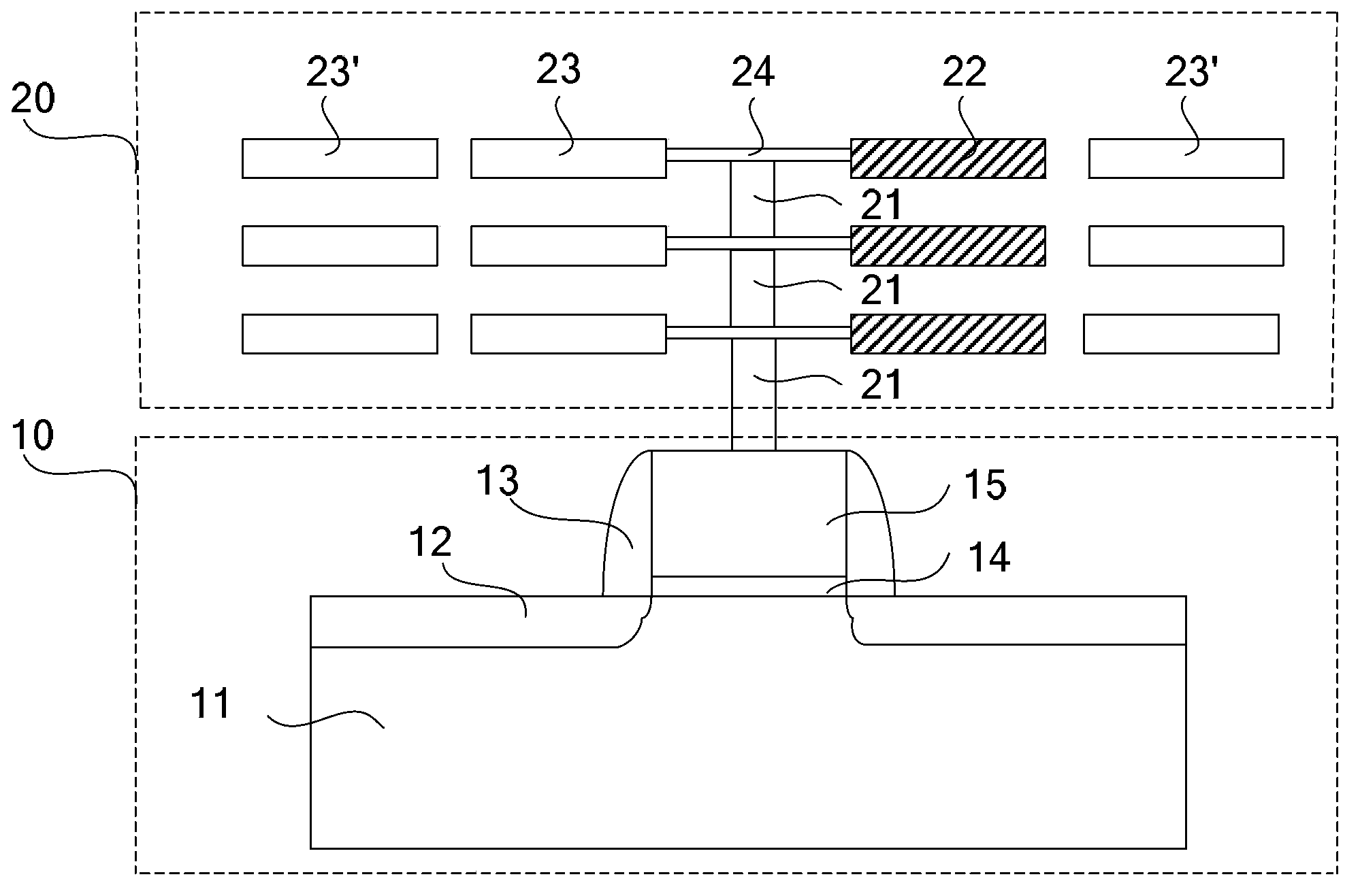
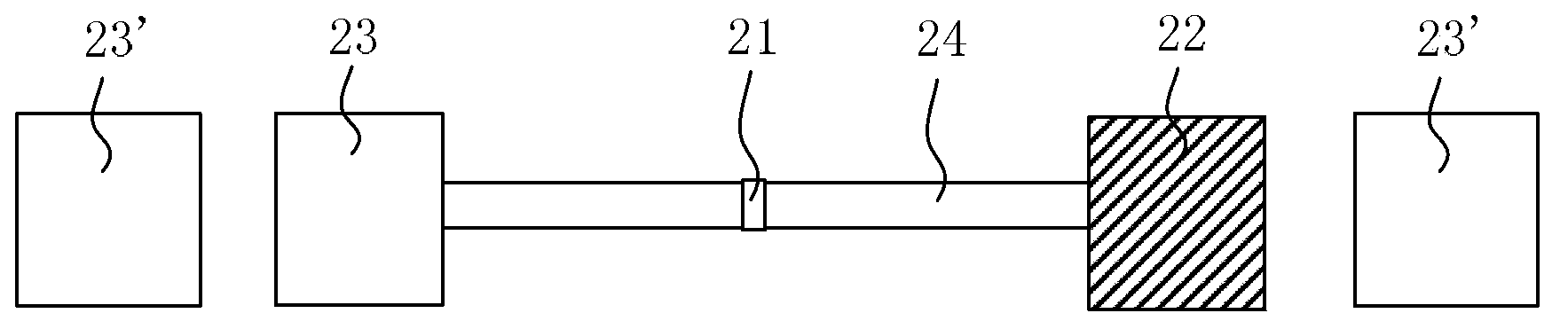
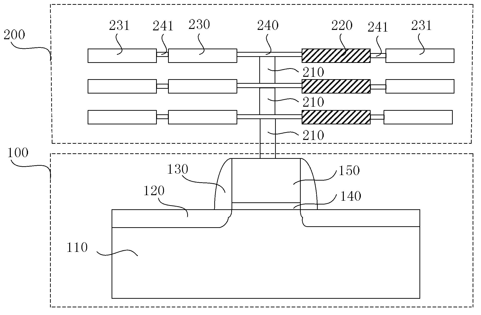
[0035] The core idea of this embodiment is to electrically connect a plurality of virtual metal bonding pads to metal bonding pads through virtual metal bonding pads, and the plurality of virtual metal bonding pads and metal bonding pads together serve as a new antenna structure for collecting charges, improving The overall area of the antenna structure is increased, thereby increasing the antenna ratio, increasing the probability of plasma-induced damage, and facilitating the rapid discovery of the cause of the plasma-induced damage to the semiconductor device.
[0036] Please refer to image 3 and Figure 4 , in this embodiment, a plasma-induced damage detection structure is proposed, including: a semiconductor device 100 , an interlayer dielectric layer (not shown in the figure), and at least one metal interconnection layer 200 formed in the interlayer dielectric layer. Wherein, the metal interconnection layer 200 includes a metal pad 230, a dummy metal pad 231, and a ...
Embodiment 2
[0050] Since the previous antenna structure is used in Embodiment 1 to be connected with the metal welding pad as a new antenna structure for collecting charges, the antenna still occupies some space on the scribing lane to some extent. In some devices, only virtual metal pads and metal pads can be used as antennas to meet the requirements. Therefore, this embodiment is improved on the basis of Embodiment 1. The original antenna structure is no longer formed, and only metal pads are formed. Welding pads and dummy metal pads, and connecting the metal pads and dummy metal pads as a new antenna structure for collecting charges.
[0051] Please refer to Figure 5 with Image 6 , in this embodiment, a plasma-induced damage detection structure for measuring plasma-induced damage is proposed, including: a semiconductor device 100; an interlayer dielectric layer (not shown in the figure) and at least A metal interconnection layer 200, wherein the metal interconnection layer 200 incl...
PUM
 Abstract
Description
Claims
Application Information
 - R&D
- Intellectual Property
- Life Sciences
- Materials
- Tech Scout
- Unparalleled Data Quality
- Higher Quality Content
- 60% Fewer Hallucinations
Browse by: Latest US Patents, China's latest patents, Technical Efficacy Thesaurus, Application Domain, Technology Topic, Popular Technical Reports.
© 2025 PatSnap. All rights reserved.Legal|Privacy policy|Modern Slavery Act Transparency Statement|Sitemap|About US| Contact US: help@patsnap.com