Ldmos tube with lateral concentration gradient in drift region and manufacturing method thereof

A concentration gradient and manufacturing method technology, applied in semiconductor/solid-state device manufacturing, electrical components, circuits, etc., can solve the problems of reduced drift region resistance, drift region energy band influence, linear current increase, etc. Hot carrier effect, effect of reducing voltage difference

Active Publication Date: 2016-11-30
SHANGHAI HUAHONG GRACE SEMICON MFG CORP
View PDF3 Cites 0 Cited by
  • Summary
  • Abstract
  • Description
  • Claims
  • Application Information

AI Technical Summary

Problems solved by technology

For PLDMOS, when the gate voltage is zero or at a lower negative gate operating potential, and the drain is connected to a higher negative operating potential, the electric field is the downward electric field that the field plate points to the drift region , the holes will be pulled downwards, and the electrons will be pushed upwards, causing electrons to be injected into the field oxygen, captured by the field oxygen and accumulated at the interface of the field oxygen to form a charge layer, which will affect the energy band of the drift region, and then affect Device characteristics, usually for PLDMOS tubes will cause the resistance of the drift region to decrease, which will increase the linear current, such as image 3 shown

Method used


Image

  • Ldmos tube with lateral concentration gradient in drift region and manufacturing method thereof
  • Ldmos tube with lateral concentration gradient in drift region and manufacturing method thereof
  • Ldmos tube with lateral concentration gradient in drift region and manufacturing method thereof

Examples


Embodiment Construction

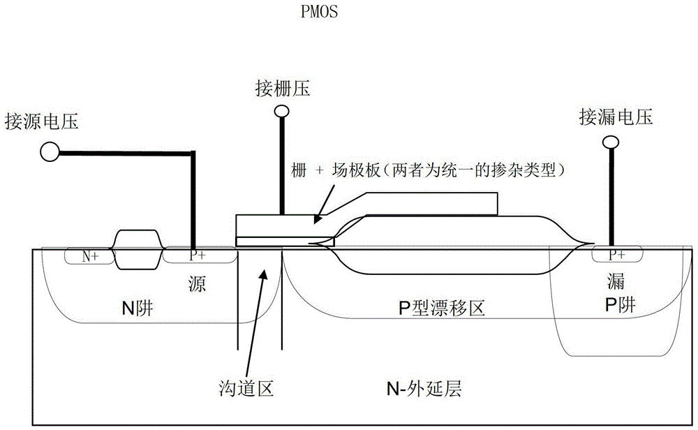
[0018] In order to have a more specific understanding of the technical content, characteristics and effects of the present invention, the PLDMOS tube is now taken as an example, and in combination with the illustrated embodiment, the LDMOS tube of the present invention and its manufacturing method are described in detail as follows:

[0019] Such as Figure 4 As shown, the gate and field plate of the PLDMOS transistor in this embodiment are composed of continuous polysilicon (poly); the gate is N-type heavily doped and connected to the gate; the field plate is divided into P-type polysilicon field plates ( Depletion region) and N-type polysilicon field plate (connection region), the size of the two parts can be flexibly adjusted according to actual needs. Among them, the doping type of the P-type polysilicon field plate is opposite to that of the gate, which is P-type lightly doped; the P-type polysilicon field plate is connected to the gate and forms a PN junction with the ga...


PUM


Abstract

The invention discloses an LDMOS transistor with a lateral concentration gradient in the drift region. The field plate of the LDMOS transistor is divided into two parts: a depletion region and a connection region. The depletion region is connected to the gate, and the doping type is opposite to that of the gate; The region is close to the drain and connected to the drain, and has the same doping type as the gate. The invention also discloses a manufacturing method of the above-mentioned LDMOS tube. The invention divides the field plate into two parts, the depletion region and the connection region with different doping types, and forms an NPN (or PNP) structure together with the gate, so that the voltage difference between the gate and the drain can be continuously distributed on the field plate In the depletion region, thereby reducing the voltage difference between the field plate and the drift region, especially the drain, and eliminating the hot carrier effect caused by the field plate.

Description

technical field [0001] The invention relates to the field of integrated circuit manufacturing, in particular to an LDMOS transistor with a lateral concentration gradient in a drift region and a manufacturing method thereof. Background technique [0002] In the design of LDMOS, how to improve the withstand voltage of the LDMOS tube has always been the core content of device design. At present, the technologies for improving the withstand voltage of LDMOS transistors mainly include optimizing the doping concentration and size of the drift region, the application of field plates, and various RESURF technologies for reducing the surface electric field intensity. Among them, the field plate technology is widely used because of its simple technology and good effect. The use of the field plate effectively reduces the peak electric field and improves the electric field distribution in the channel and the drift region under the field oxygen. [0003] The current field plate structu...

Claims


Application Information

Patent Timeline
Patent Type & Authority Patents(China)
IPC IPC(8): H01L29/78H01L29/40H01L21/336H01L21/28H01L21/265
Inventor 杨文清赵施华邢军军
Owner SHANGHAI HUAHONG GRACE SEMICON MFG CORP
Why Eureka
Try Eureka