Light emitting device inserted with current homogenizing structure and manufacturing method thereof

A technology for light-emitting devices and manufacturing methods, which is applied in the direction of electrical components, semiconductor devices, circuits, etc., can solve problems such as reducing the working life of devices, limiting the rated power of devices, and breakdown of light-emitting devices, so as to reduce light shading and uniform current distribution , to enhance the effect of lateral flow

Inactive Publication Date: 2014-05-21
INST OF SEMICONDUCTORS - CHINESE ACAD OF SCI
View PDF3 Cites 2 Cited by
  • Summary
  • Abstract
  • Description
  • Claims
  • Application Information

AI Technical Summary

Problems solved by technology

The current edge effect can easily cause local overheating and breakdown of the light-emitting device, which will reduce the working life of the device and limit the rated power of the device
For ordinary power diodes, the current collector effect is a common problem.

Method used


Image

  • Light emitting device inserted with current homogenizing structure and manufacturing method thereof
  • Light emitting device inserted with current homogenizing structure and manufacturing method thereof
  • Light emitting device inserted with current homogenizing structure and manufacturing method thereof

Examples


Example Embodiment

[0024] In order to make the objectives, technical solutions, and advantages of the present invention clearer, the following further describes the present invention in detail in conjunction with specific embodiments and with reference to the accompanying drawings.

[0025] In the drawings, for convenience and clarity of explanation, the thickness or size of each layer may be enlarged, reduced, or schematically shown, and the size of each constituent part does not or may not necessarily reflect its actual size.
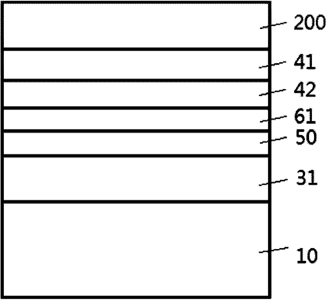
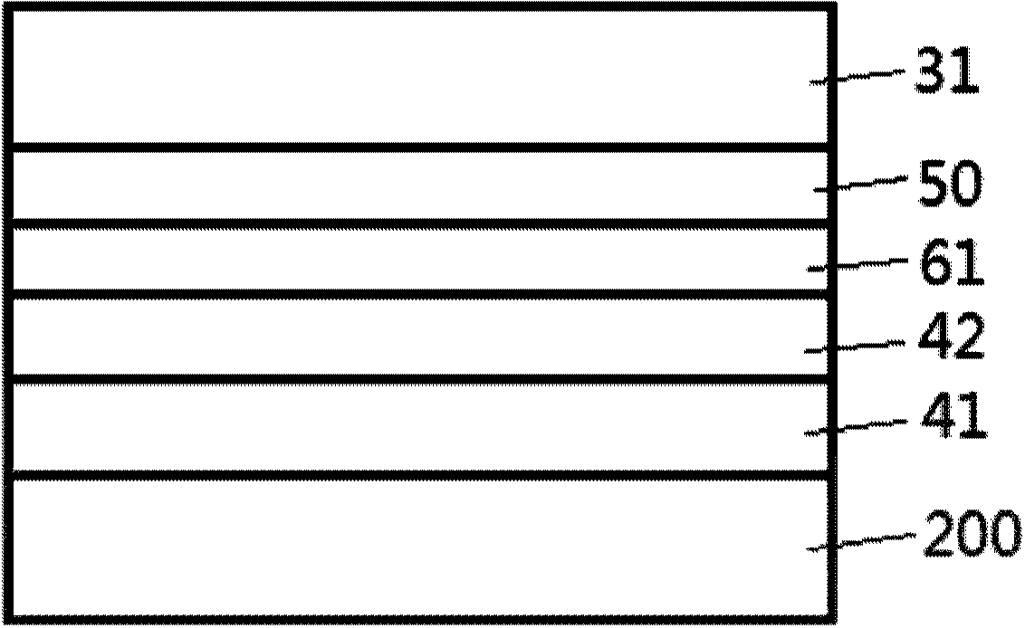
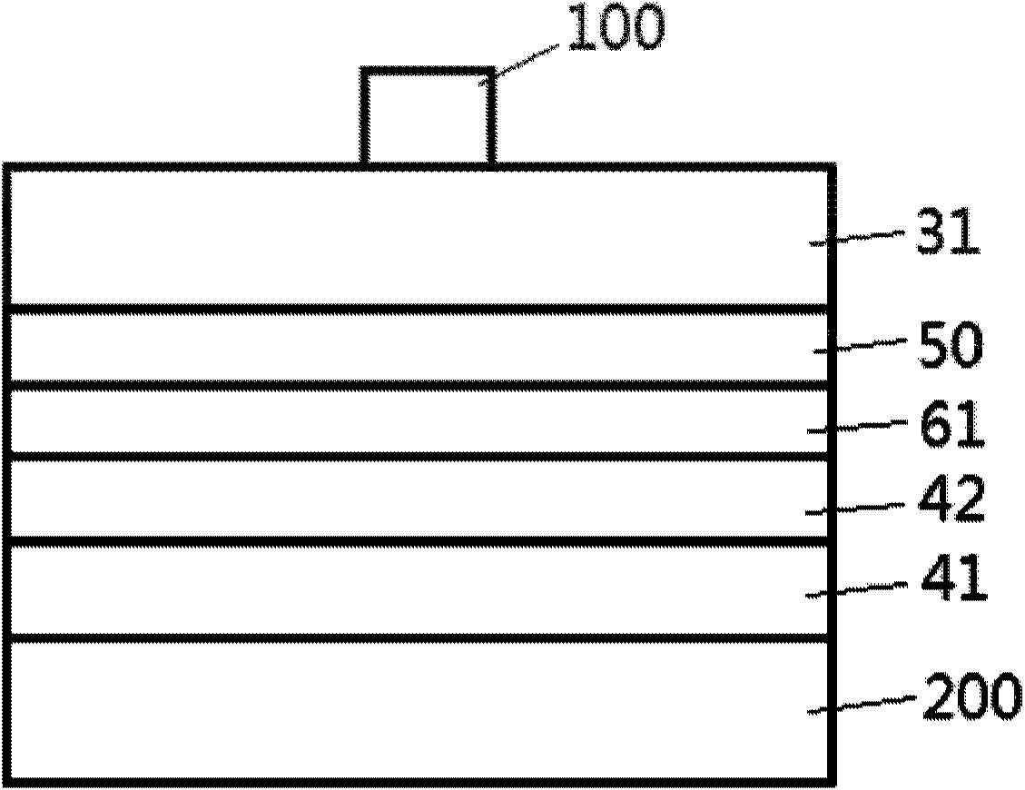
[0026] Hereinafter, the method of manufacturing the light emitting device according to the first embodiment will be described in detail with reference to the accompanying drawings. Figure 1 to Figure 3 It is a process flow chart of manufacturing a light-emitting device with a homogenized current structure inserted according to the first embodiment of the present invention.

[0027] Reference figure 1 , An n-type semiconductor layer 31, an active layer 50, a second degenerate p...


PUM


Abstract

The invention discloses a light emitting device inserted with a current homogenizing structure and a manufacturing method thereof. The light emitting device inserted with the current homogenizing structure comprises a first electrode layer, a p type degeneration semiconductor layer on the first electrode layer, an n type degeneration semiconductor layer on the p type degeneration semiconductor layer, a p type semiconductor layer on the n type degeneration semiconductor layer, an active layer on the p type semiconductor layer, an n type semiconductor layer on the active layer, and a second electrode layer on the n type semiconductor layer. By adopting the light emitting device, the current distribution uniformity during working of the semiconductor device can be improved effectively, the photo, electrical and thermal performance of the semiconductor device is improved, and the service life is prolonged.

Description

technical field [0001] The invention belongs to the technical field of semiconductors, in particular to a light-emitting device inserted with a homogenizing current structure and a manufacturing method thereof. Background technique [0002] The electrode area of ​​the light-emitting surface of the light-emitting device always only occupies a small part of its corresponding working area. The current injected by the device is likely to be concentrated near the electrode and cannot be effectively spread throughout the entire device, resulting in injection into the junction area. The current distribution is uneven, this effect is called the current edge effect. The current edge effect can easily cause local overheating of the light-emitting device and cause breakdown, which will reduce the working life of the device and limit the rated power of the device. For ordinary power diodes, the current collector effect is a common problem. When designing the device structure and electr...

Claims


Application Information

Patent Timeline
IPC IPC(8): H01L33/14H01L33/00
CPCH01L33/14H01L33/145
Inventor 郭恩卿伊晓燕刘志强陈宇王军喜李晋闽
Owner INST OF SEMICONDUCTORS - CHINESE ACAD OF SCI
Why Eureka
Try Eureka