Unlock instant, AI-driven research and patent intelligence for your innovation.

Manufacturing method of semiconductor device test sample

A manufacturing method and a technology for testing samples, which are applied in the semiconductor field, can solve problems such as floating gate short circuit, FLASH memory failure, etching, etc., and achieve the effect of small aspect ratio

Active Publication Date: 2014-05-28
SHANGHAI HUAHONG GRACE SEMICON MFG CORP
View PDF5 Cites 4 Cited by
  • Summary
  • Abstract
  • Description
  • Claims
  • Application Information

AI Technical Summary

Problems solved by technology

[0005] like figure 2 As shown, in the subsequent steps, it is necessary to form a second spacer 08 on the sidewall of the gate structure, and then form a lead 09 between adjacent second sidewalls 08 in the trench 07. etch residue defects such as figure 2 As shown in the middle circle, it may cause the lead 09 to be short-circuited with the floating gate of the gate structure, causing the FLASH memory to fail
[0006] In order to ensure the quality of the FLASH memory, after etching the second polysilicon layer 02, the ONO layer 03, and the first polysilicon layer 04, it is necessary to conduct an on-line inspection of the possible etching residue defects in the trench 07. Detection, the object of online monitoring is the test sample of the memory formed in the wafer test area. The test sample of the existing memory is usually formed completely synchronously with the FLASH memory in the device area, and is consistent with the shape and size of the FLASH memory in the device area. Consistently, because the aspect ratio of trench 07 is too large in the test sample formed in this way, it is difficult for online wafer inspection equipment to capture the defect of etching residue in trench 07

Method used


Image

  • Manufacturing method of semiconductor device test sample
  • Manufacturing method of semiconductor device test sample
  • Manufacturing method of semiconductor device test sample

Examples


Embodiment Construction

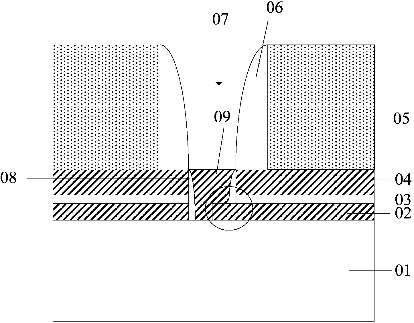
[0030] In existing semiconductor device test samples, if defects such as etching residues occur in trenches with a high aspect ratio, it is difficult for wafer inspection equipment to capture the above defects, which will easily cause batches of wafers to be scrapped due to defects , causing losses.

[0031] In order to solve the above technical problems, the present invention provides a method for manufacturing a test sample of a semiconductor device, so that the wafer inspection equipment can more sensitively capture the defects of etching residues in the gap online, and monitor such defects in time. Reduce the probability of semiconductor device failure.

[0032] In order to make the above objects, features and advantages of the present invention more comprehensible, specific embodiments of the present invention will be described in detail below in conjunction with the accompanying drawings.

[0033] In the following embodiments, the method for making a semiconductor devic...


PUM

PropertyMeasurementUnit
Thicknessaaaaaaaaaa
Thicknessaaaaaaaaaa
Thicknessaaaaaaaaaa

Abstract

The invention provides a manufacturing method of a semiconductor device test sample. The manufacturing method comprises the steps as follows: a substrate is provided; a to-be-etched layer is formed on the substrate; an insulating layer is formed on the to-be-etched layer; a groove for exposing a conductive material layer is formed in the insulating layer; the insulating layer is taken as a mask, the to-be-etched layer exposed out of the groove is removed to form a gap; and the insulating layer is removed. After the insulating layer is removed, the groove above the gap is also removed, and if etching residues are generated in the gap, wafer detection equipment can flexibly capture the etching residue defect of the gap on line and timely monitors the defect due to the fact that a depth-to-width ratio of the gap is smaller than that of the groove in the insulating layer.

Description

technical field [0001] The invention relates to the field of semiconductors, in particular to a method for manufacturing a test sample of a semiconductor device. Background technique [0002] In the manufacturing process of semiconductor devices, defects on wafers are unavoidable. In order to improve the yield rate of semiconductor devices, in the manufacturing process, there are usually multiple In-Line Monitoring (ILM) processes to detect defects in time during the manufacturing process and improve the process in time, so that the subsequent wafers Yield is improved. [0003] In the current process, online wafer inspection equipment is usually used to detect the defects of the wafer. The specific detection principle is: use the detection beam to scan the surface of the wafer to be tested, and process the beam reflected from the wafer surface to obtain the wafer defect. Defect data for a circular surface. However, this method is more suitable for the situation where defe...

Claims


Application Information

Patent Timeline
IPC IPC(8): G01N1/28H01L21/66
Inventor 胡淼袁力韩超
Owner SHANGHAI HUAHONG GRACE SEMICON MFG CORP
Features
  • R&D
  • Intellectual Property
  • Life Sciences
  • Materials
  • Tech Scout
  • Unparalleled Data Quality
  • Higher Quality Content
  • 60% Fewer Hallucinations
Learn More