Low-temperature wafer bonding method
A wafer bonding, low temperature technology, applied in instruments, welding equipment, optomechanical equipment, etc., can solve the problems of low bonding strength, limitation, limited use temperature of devices, etc., to achieve the effect of high efficiency and avoid damage
- Summary
- Abstract
- Description
- Claims
- Application Information
AI Technical Summary
Problems solved by technology
Method used
Image

Examples
Embodiment Construction
[0029] In order to make the object, technical solution and advantages of the present invention clearer, the present invention will be described in further detail below in conjunction with specific embodiments and with reference to the accompanying drawings.
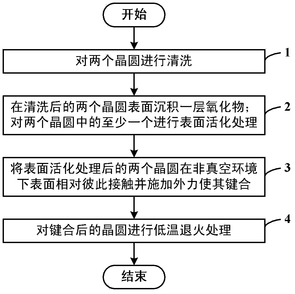
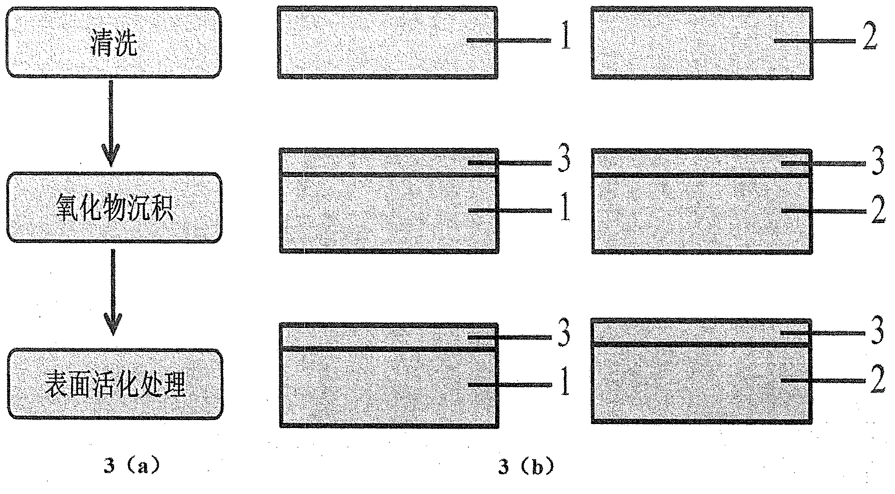
[0030] This low-temperature wafer bonding method provided by the present invention first cleans the two wafers, then deposits a thin oxide layer on the bonding regions of the two wafers respectively, and removes the oxide layer deposited on at least one of the wafers. Surface activation treatment is carried out, and the oxide layers of the two processed wafers are relatively pasted together, and finally sent to the bonding machine to apply extrusion force, so as to realize the bonding of the two wafers.
[0031] like figure 1 as shown, figure 1 A flow chart of a method for low temperature wafer bonding according to an embodiment of the present invention is shown, and the method includes the following steps:
[0032] Ste...
PUM
 Abstract
Description
Claims
Application Information
 - Generate Ideas
- Intellectual Property
- Life Sciences
- Materials
- Tech Scout
- Unparalleled Data Quality
- Higher Quality Content
- 60% Fewer Hallucinations
Browse by: Latest US Patents, China's latest patents, Technical Efficacy Thesaurus, Application Domain, Technology Topic, Popular Technical Reports.
© 2025 PatSnap. All rights reserved.Legal|Privacy policy|Modern Slavery Act Transparency Statement|Sitemap|About US| Contact US: help@patsnap.com