Assembly structure and method of an optical device
An optical device and assembly structure technology, applied in optical components, optics, installation and other directions, can solve the problems of not too thin wall thickness, easy to generate large stress, high cost, improve temperature stability, efficient assembly and fixation, reduce effect of stress
- Summary
- Abstract
- Description
- Claims
- Application Information
AI Technical Summary
Problems solved by technology
Method used
Image
Examples
Embodiment Construction
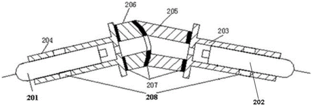
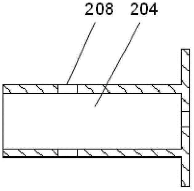
[0029] Such as figure 2 , image 3 , Figure 4 As shown, the optical components in this embodiment are described by taking a fiber collimator as an example, which includes a first optical device 201 and a second optical device 202, a ball joint with a light hole, a secondary concave ball joint 205 and a convex ball Joint 206, the first optical device 201 is fixed in the first T-shaped sleeve 204, the second optical device 202 is fixed in the second T-shaped sleeve 203, the first T-shaped sleeve 204 The diameter of the inner hole of the second T-shaped sleeve 203 is slightly larger than the outer diameter of the first optical device 201 and the second optical device 202, and a loose fit can be achieved through positive and negative tolerances. The first T-shaped sleeve 204 and The T surface end of the second T-shaped sleeve 203 is connected by the concave ball joint 205 and the convex ball joint 206 of the ball joint pair, and the concave ball joint 205 and the convex ball j...
PUM
 Abstract
Description
Claims
Application Information


