Electronic picture photoreceptor and image forming device
An electrophotographic and photoreceptor technology, applied in the fields of electrophotographic photoreceptors and image forming devices, can solve problems such as difficulty in obtaining sensitivity characteristics
- Summary
- Abstract
- Description
- Claims
- Application Information
AI Technical Summary
Problems solved by technology
Method used
Image
Examples
no. 1 approach
[0019] The electrophotographic photoreceptor according to the first embodiment of the present invention relates to a photosensitive layer formed on a conductive substrate, the photosensitive layer contains a charge transport material, and the charge transport material contains an iminoquinone derivative represented by the following general formula (1). Electrophotographic photoreceptors as electron transport materials.
[0020]
[0021] (In general formula (1), R 1 and R 2 are selected from a hydrogen atom, a halogen atom, a nitro group, an alkyl group having 1 to 12 carbon atoms, an aryl group having 6 to 12 carbon atoms which may be substituted by an alkyl group having 1 to 12 carbon atoms, and a carbon A group consisting of an aralkyl group with 6 to 12 atoms, a cycloalkyl group with 3 to 10 carbon atoms, and an alkoxy group with 1 to 6 carbon atoms, R 3 and R 4 are selected from a hydrogen atom, an alkyl group having 1 to 12 carbon atoms, an aryl group having 6 to 12...
no. 2 approach
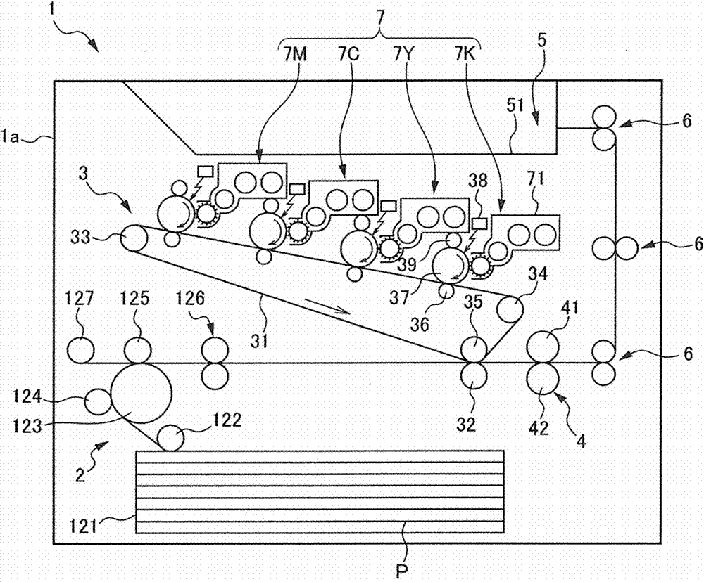
[0096] A second embodiment of the present invention relates to an image forming apparatus including: an image carrier; a charging unit for charging the surface of the image carrier; and an exposure unit for exposing the charged surface of the image carrier, thereby an electrostatic latent image is formed on the surface of the image carrier; a developing section for developing the electrostatic latent image into a toner image; and a transfer section for transferring the toner image from the image carrier to a transferred body , the electrophotographic photoreceptor according to the first embodiment of the present invention is used as an image carrier.
[0097] In the image forming apparatus according to the second embodiment of the present invention, structural units other than the image carrier, such as the charging unit, the exposure unit, the developing unit, and the transfer unit, can be obtained from those used in conventional image forming apparatuses. Appropriate choice ...
Embodiment 1~10、 and comparative example 1、2
[0126]
[0127]Using the hole transport material, electron transport material and charge generation material described in Table 1, single-layer electrophotographic photoreceptors were prepared according to the following method, and the sensitivity of the single-layer electrophotographic photoreceptors was evaluated.
[0128] (Preparation of Coating Solution)
[0129] 80 parts by mass of the hole transport material (HTM-1), 50 parts by mass of the electron transport material of the type described in Table 1, and the charge generation material of the type described in Table 1 (X-type metal-free phthalocyanine (x-H 2 Pc) or titanium phthalocyanine (Y-TiOPc)) 5 parts by mass, binder resin (polycarbonate) 100 parts by mass, and solvent (tetrahydrofuran) 800 parts by mass were put into a ball mill, mixed and dispersed for 50 hours and A coating liquid for a single-layer photoreceptor was prepared.
[0130] (Production of single-layer photoreceptor)
[0131] After coating the obt...
PUM
| Property | Measurement | Unit |
|---|---|---|
| Film thickness | aaaaa | aaaaa |
| Thickness | aaaaa | aaaaa |
Abstract
Description
Claims
Application Information


