Reverse-conducting type insulated gate bipolar transistor structure and manufacturing method thereof

A technology of bipolar transistors and insulated gates, which is applied in the field of reverse conduction insulated gate bipolar transistors and its preparation, can solve problems such as poor reverse recovery characteristics, and achieve the effect of high collector doping concentration

Active Publication Date: 2014-06-11
INST OF MICROELECTRONICS CHINESE ACAD OF SCI +2
View PDF4 Cites 2 Cited by
  • Summary
  • Abstract
  • Description
  • Claims
  • Application Information

AI Technical Summary

Problems solved by technology

[0005] The technical problem to be solved by the present invention is to provide a reverse conduction insulated gate bipolar transistor structure and its preparation method, which solves the technical problem of poor reverse recovery characteristics of the reverse conduction insulated gate bipolar transistor in the prior art

Method used


Image

  • Reverse-conducting type insulated gate bipolar transistor structure and manufacturing method thereof
  • Reverse-conducting type insulated gate bipolar transistor structure and manufacturing method thereof
  • Reverse-conducting type insulated gate bipolar transistor structure and manufacturing method thereof

Examples


Embodiment Construction

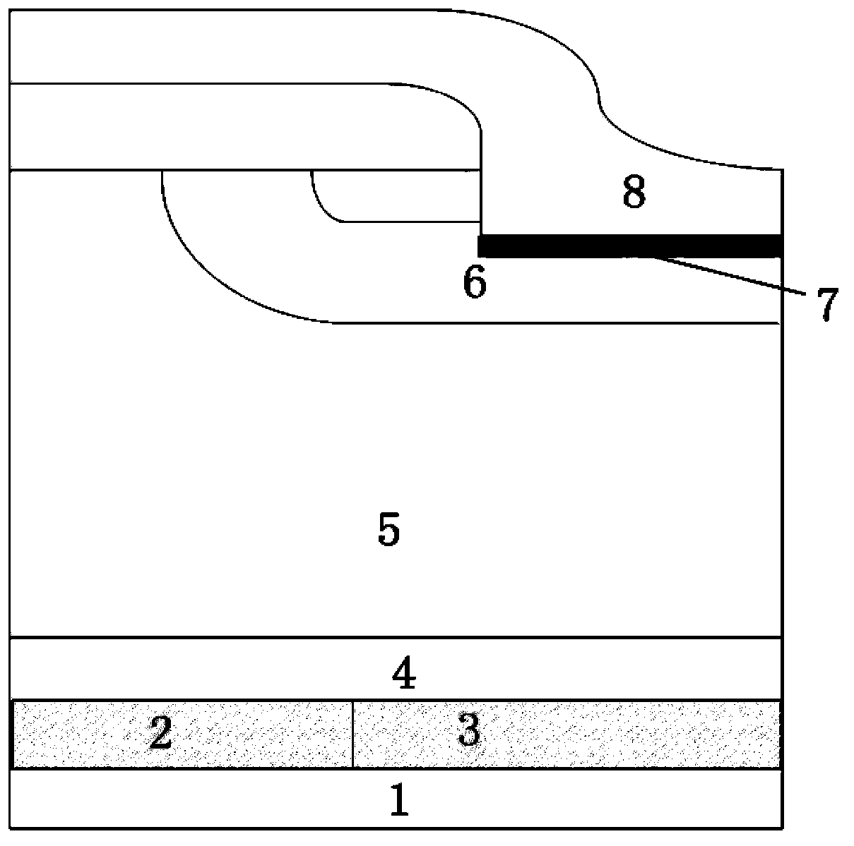
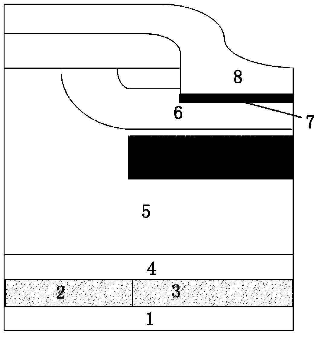
[0023] see image 3 , a reverse conduction insulated gate bipolar transistor structure provided by an embodiment of the present invention, comprising a collector 1, a second P+ doped layer 2, an N+ doped layer 3, an N+ buffer layer 4, an N-base region 5, a P -base 6, first P+ doped layer 7 and emitter 8; wherein, N+ buffer layer 4, N-base region 5 and P-base 6 form a diode structure, and the top of N-base region 5 is P-base 6, Below the N-base region 5 is an N+ buffer layer 4, above the P-base 6 is a first P+ doped layer 7, and above the first P+ doped layer 7 is formed an emitter 8, a reverse conduction insulated gate bipolar transistor There are second P+ doped layer 2 and N+ doped layer 3 on the back side of the backside, the collector electrode 1 is formed under the second P+ doped layer 2 and N+ doped layer 3, and the N-base region 5 close to the P-base 6 There is a local lifetime control region 9 above, and the introduction of a deep level recombination center of carrie...


PUM


Abstract

The invention discloses a reverse-conducting type insulated gate bipolar transistor structure and a manufacturing method of the reverse-conducting type insulated gate bipolar transistor structure, and belongs to the technical field of semiconductor power devices. The reverse-conducting type insulated gate bipolar transistor structure comprises a collector, a second P+ doped layer, an N+ doped layer, an N+ buffer layer, an N- base region, a P- substrate, a first P+ doped layer and an emitting electrode, wherein the P- substrate is arranged on the top of the N- base region, the N+ buffer layer is arranged at the bottom of the N- base region, the first P+ doped layer is arranged on the top of the P- substrate, the emitting electrode is formed on the top of the first P+ doped layer, the second P+ doped layer and the N+ doped layer are arranged on the reverse side of a reverse-conducting type insulated gate bipolar transistor, the collector is formed at the bottom of the second P+ doped layer and the bottom of the N+ doped layer, and a local area service life control area is arranged on the portion, close to the P- substrate, of the N- base region. According to the reverse-conducting type insulated gate bipolar transistor structure and the manufacturing method of the reverse-conducting type insulated gate bipolar transistor structure, the reverse recovery characteristic of the reverse-conducting type IGBT in the diode mode can be remarkably improved on the basis that the manufacturing cost of the IGBT is not remarkably increased.

Description

technical field [0001] The invention belongs to the technical field of semiconductor power devices, and in particular relates to a reverse conduction type insulated gate bipolar transistor structure and a preparation method thereof. Background technique [0002] When a traditional insulated gate bipolar transistor (IGBT) is subjected to a reverse bias, the collector junction is reversed and cannot be turned on. Therefore, the insulated gate bipolar transistor is often used together with an anti-parallel fast recovery diode, and the inductive load of the insulated gate bipolar transistor is provided with a current discharge channel through the fast recovery diode. Most single transistors and modules of IGBTs in practical applications are packaged together by IGBT chips and fast recovery diode chips. Reverse conduction insulated gate bipolar transistor is a new type of insulated gate bipolar transistor device in the world. It skillfully integrates the traditional insulated ga...

Claims


Application Information

Patent Timeline
Patent Type & Authority Applications(China)
IPC IPC(8): H01L29/739H01L29/06H01L21/331H01L21/265
CPCH01L21/26506H01L29/0821H01L29/1004H01L29/16H01L29/161H01L29/66325H01L29/7393
Inventor 胡爱斌朱阳军田晓丽张文亮
Owner INST OF MICROELECTRONICS CHINESE ACAD OF SCI
Why Eureka
Try Eureka