Equivalent circuit and simulation method for high-voltage LDMOS device

A technology of equivalent circuit and simulation method, applied in the fields of instruments, electrical digital data processing, special data processing applications, etc., can solve the problem of inability to describe the substrate current of the lightly impurity drift region in LDMOS, and achieve the effect of improving the simulation accuracy

Inactive Publication Date: 2014-06-18
SHANGHAI HUAHONG GRACE SEMICON MFG CORP
View PDF2 Cites 8 Cited by
  • Summary
  • Abstract
  • Description
  • Claims
  • Application Information

AI Technical Summary

Problems solved by technology

[0004] At present, standard simulation models such as BSIM (Berkeley Short channel Insulated gate field effect transistor Model Berkeley Short Channel Insulated Gate Field Effect Transistor Model) and PS

Method used


Image

  • Equivalent circuit and simulation method for high-voltage LDMOS device
  • Equivalent circuit and simulation method for high-voltage LDMOS device
  • Equivalent circuit and simulation method for high-voltage LDMOS device

Examples


Embodiment Construction

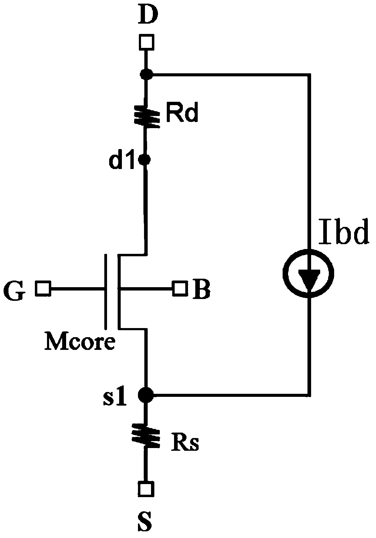
[0040] The equivalent circuit and simulation method of the high-voltage LDMOS device described in the invention are suitable for SPICE simulation. Its equivalent circuit structure is as image 3 As shown, it is composed of components that characterize some special structural characteristics of high-voltage LDMOS devices on the basis of the traditional MOSFET simulation model BSIM. The traditional BSIM model contains only image 3 The MOSFET shown is a source-drain symmetrical or asymmetrical MOSFET, and its connection relationship with other external components is as follows:

[0041] The drain of the MOSFET is connected to the first end of a first resistor Rd;

[0042] The source of the MOSFET is connected to the first end of a second resistor Rs;

[0043] Two ends of a current source Ibd are respectively connected to the second end of the first resistor Rd and the source of the MOSFET;

[0044] The gate of the MOSFET, the second end of Rd, and the second end of Rs are res...


PUM


Abstract

The invention discloses an equivalent circuit and a simulation method for a high-voltage LDMOS device. In a high-voltage LDMOS device structure, the substrate current of a lightly-doped drift region is obviously different from that of the traditional intrinsic MOSFET, and a standard SPICE BSIM3 model is incapable of accurately simulating the substrate current of the lightly-doped drift region of the high-voltage LDMOS. According to the equivalent circuit and the simulation method disclosed by the invention, the collision ionization current of the lightly-doped drift region is accurately simulated by externally connecting a current source, a source equivalent resistor and a drain equivalent resistor, thus improving simulation accuracy and reducing a circuit design cycle.

Description

technical field [0001] The invention relates to design simulation of semiconductor devices, in particular to an equivalent circuit of a high-voltage LDMOS device, and also relates to a simulation method of the high-voltage LDMOS device. Background technique [0002] Because LDMOS (Laterally Diffused Metal Oxide Semiconductor) has high breakdown voltage, low on-resistance and high process integration, LDMOS is widely used in power integrated circuits and RF circuit design. In the design of these circuits, an accurate physical LDMOS model is one of the key factors for a successful design. LDMOS device structure such as figure 1 As shown, the source is located in the P-type body region, and the drain lightly doped N-type well is also called the LDMOS drift region. The depleted region is resistant to high voltage, and the gate polysilicon covers from the gate oxide to part of the field oxygen on the N-type well of the lightly doped drain. The part of the gate polysilicon locat...

Claims


Application Information

Patent Timeline
IPC IPC(8): G06F17/50
Inventor 武洁
Owner SHANGHAI HUAHONG GRACE SEMICON MFG CORP
Why Eureka
Try Eureka