
Dry etching method

A technology of dry etching and photoresist, which is applied in the direction of electrical components, semiconductor/solid-state device manufacturing, circuits, etc., can solve the problems of limited line edge roughness and complicated conditions, and achieve optimal dry etching conditions, The effect of improving uniformity

Inactive Publication Date: 2014-06-18
WUHAN XINXIN SEMICON MFG CO LTD
View PDF6 Cites 1 Cited by
  • Summary
  • Abstract
  • Description
  • Claims
  • Application Information

AI Technical Summary

Problems solved by technology

However, the degree of roughness of the edge of the line is limited by selecting better materials such as photoresist and optimizing the photolithography process conditions, and the required conditions are complicated.

Method used


Image

  • Dry etching method
  • Dry etching method
  • Dry etching method

Examples


Embodiment Construction

[0020] The principles and features of the present invention are described below in conjunction with the accompanying drawings, and the examples given are only used to explain the present invention, and are not intended to limit the scope of the present invention.

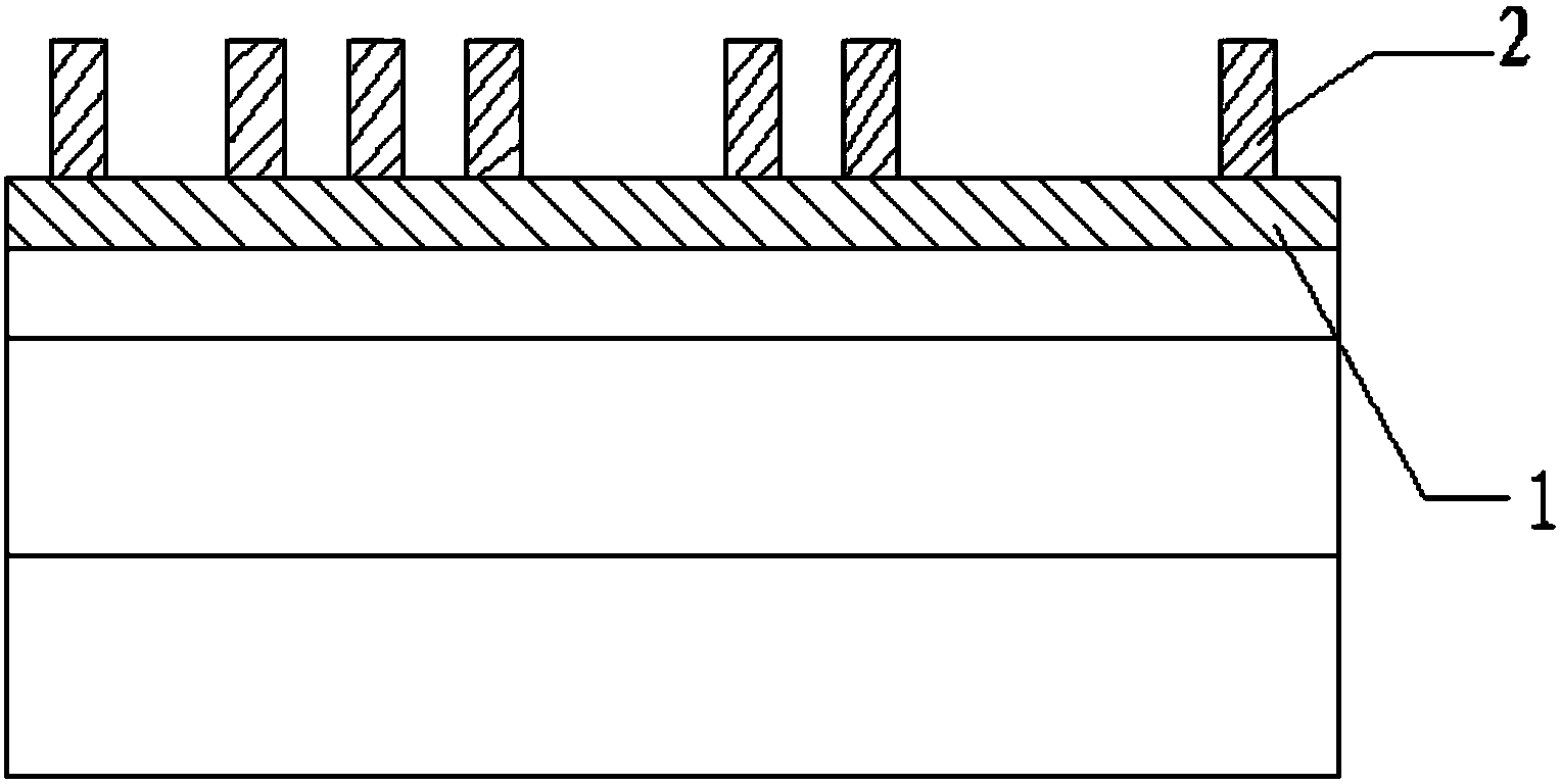
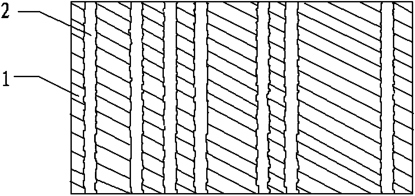
[0021] Such as figure 1 , figure 2 As shown, after the photoresist 2 on the wafer 1 is exposed and developed, the roughness of the photoresist 2 itself is relatively high, such as figure 2 The edge of the photoresist 2 represented by the rough edge lines in the middle, such roughness has a serious impact on the later processing of the wafer and the quality of the wafer.

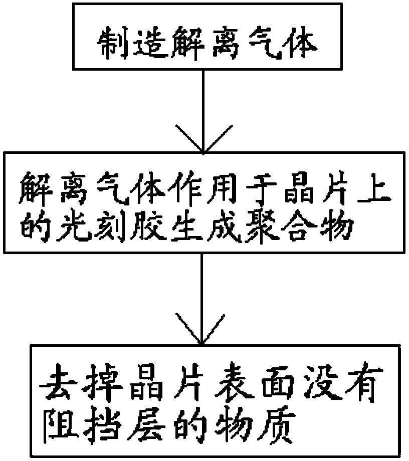
[0022] to solve figure 1 , figure 2 In view of the problem of the roughness of the photoresist itself after exposure and development, the present invention provides a dry etching method, such as image 3 Shown, a kind of dry etching method, at first manufacture dissociation gas, adopt high-frequency plasma method to dissociate gas; The gas c...


PUM


Abstract

The invention relates to a dry etching method. The dry etching method comprises the following steps that firstly, dissociation gas is manufactured; secondly, photoresist reaction is conducted on the dissociation gas and the surface of a wafer with photoresist, and a layer of dense polymer is formed on the surface of the photoresist; thirdly, matter without blocking layers on the surface of the wafer is removed by means of physical or / and chemical reaction between plasma generated in the dissociation gas and the wafer. According to the method, by optimizing dry etching conditions, the dissociation gas and the photoresist on the surface of the wafer react on the primary stage of dry etching, the dense polymer which is relatively hard relative to the photoresist is formed, the polymer itself can not cause key size deviation, line edge roughness generated in the photoetching step can be restored to a certain degree, and therefore the line edge roughness of the wafer processed in the dry etching method can be improved.

Description

technical field [0001] The invention relates to an etching method, in particular to a dry etching method. Background technique [0002] With the continuous improvement of the integration density of semiconductor chips, the critical dimensions are getting smaller and smaller, and the challenges related to the pattern transfer related process methods are getting higher and higher. The dry etching process is used as the pattern transfer defined by the photolithography step. In the implementation process of the key process method on the chip, not only the difference in key dimensions caused by the photolithography process must be overcome, but even the roughness of the photoresist itself caused by exposure and development must be resolved as much as possible. As process nodes get more and more advanced, this part becomes more and more important. In the prior art, the roughness of the line edge is reduced as much as possible by selecting better materials such as photoresist and ...

Claims


Application Information

Patent Timeline
Patent Type & Authority Applications(China)
IPC IPC(8): H01L21/027
CPCH01L21/0331H01L21/31058
Inventor 黄海洪齐元
Owner WUHAN XINXIN SEMICON MFG CO LTD
Learn More