IGBT and manufacturing method thereof

A semiconductor and shallow well technology, applied in the field of semiconductor device manufacturing technology, can solve problems such as latch-up effect, weak anti-latch-up ability, and small current

Inactive Publication Date: 2014-06-18
SHANGHAI LIANXING ELECTRONICS +2
View PDF0 Cites 4 Cited by
  • Summary
  • Abstract
  • Description
  • Claims
  • Application Information

AI Technical Summary

Problems solved by technology

However, in fact, when the above-mentioned IGBT is working, when the hole current reaches a certain value, the IGBT cannot be turned off after it is turned on, and a latch-up e

Method used


Image

  • IGBT and manufacturing method thereof
  • IGBT and manufacturing method thereof
  • IGBT and manufacturing method thereof

Examples


Embodiment Construction

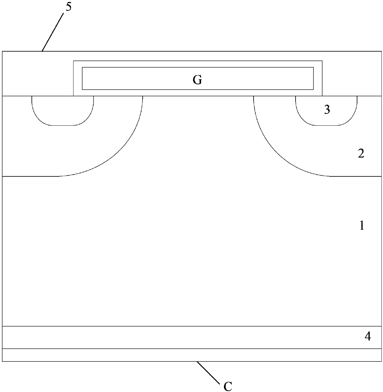
[0038] As mentioned in the background, the existing IGBT has low latch-up current and weak latch-up resistance.

[0039] refer to figure 1 ,exist figure 1 In the shown IGBT, its N + Source region 3, P-type well region 2, N - drift region and P + Collector 4 constitutes a parasitic NPNP thyristor. The NPNP thyristor includes: NPN transistor Q1 (N + Source region 3-P-type well region 2-N-drift region) and PNP transistor Q2 (P-type well region 2-N- - Drift Zone-P + collector area 4). IGBT has three PN junctions: N + PN junction J3 between source region 3 and P-type well region 2, P-type well region 2 and N - PN junction J2 between the drift region, N - Drift region and P + PN junction J1 between collector regions 4 . Wherein, the drift region is a part of the semiconductor substrate that does not include the well region, the source region and the collector region.

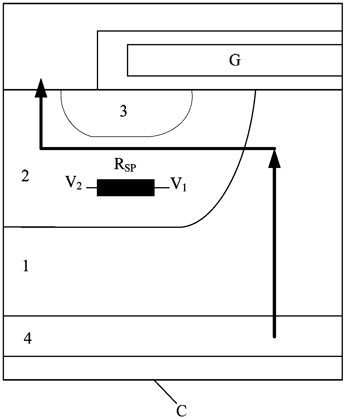
[0040] refer to figure 2 , figure 2 for figure 1 Schematic diagram of the equivalent analysis of ...


PUM

PropertyMeasurementUnit
Lengthaaaaaaaaaa
Depthaaaaaaaaaa

Abstract

The invention discloses an IGBT and a manufacturing method thereof. The IGBT includes: a gate structure located on an upper surface of a semiconductor substrate; a well region, a source region and a shallow well region located inside the upper surface of the semiconductor substrate, the well region being internally provided with the source region, upper surfaces of the well region, the source region and the shallow well region being flush with the upper surface of the semiconductor substrate, and the well region and the shallow well region being not in contact and the same in doping type; a source electrode located on surfaces of the well region, the shallow well region and the source region; and a reverse side structure located on a lower surface of a semiconductor, and the reverse side structure including a collector region. When the IGBT works, a part of a hole current can pass the collector region, a drift region and the well region, and flow into the source electrode, and a part of the hole currents can pass the collector region, the drift region and the shallow region, and flow into the source electrode. Thus, the shallow well region provides an extra current channel for the IGBT to shunt the hole current, thereby improving a latching current of the IGBT, and enhancing an anti-latching capability of the IGBT.

Description

technical field [0001] The present invention relates to the technical field of manufacturing technology of semiconductor devices, and more specifically, relates to an IGBT and a manufacturing method thereof. Background technique [0002] Insulated Gate Bipolar Transistor (IGBT for short) is a composite fully-controlled voltage-driven power semiconductor device composed of a bipolar transistor (BJT) and an insulated gate field effect transistor (MOSFET), and has a MOSFET Due to the high input impedance of the device and the high-speed switching characteristics of the power transistor (Giant Transistor, GTR for short), the IGBT, as a necessary switching device, is widely used in circuit structures such as frequency converters and inverters. [0003] refer to figure 1 , figure 1 It is a schematic structural diagram of an IGBT with a planar gate structure, including: N-type lightly doped (N - ) semiconductor substrate 1; located at N - The gate structure and the source struc...

Claims


Application Information

Patent Timeline
IPC IPC(8): H01L29/739H01L29/06H01L21/331
CPCH01L29/7398H01L29/0684H01L29/66333
Inventor 谈景飞朱阳军胡爱斌张文亮王波
Owner SHANGHAI LIANXING ELECTRONICS
Why Eureka
Try Eureka