Supercharge Your Innovation With Domain-Expert AI Agents!

Method for growing nitride epitaxial layer on silicon substrate and semiconductor device thereof

A technology of nitride epitaxial layer and silicon substrate, which is applied in the direction of semiconductor devices, electrical components, circuits, etc., can solve the problems of unsatisfactory effect, affecting the crystal quality uniformity of the epitaxial layer, and the difficulty of the aluminum nitride layer process, etc., to achieve Solve cracks and dislocations, improve crystal quality, and enhance device performance

Active Publication Date: 2016-12-21
DEPOSITION EQUIP & APPL SHANGHAI LTD
View PDF1 Cites 0 Cited by
  • Summary
  • Abstract
  • Description
  • Claims
  • Application Information

AI Technical Summary

Problems solved by technology

For example, preparing a regular square pattern on a silicon substrate and inserting an aluminum nitride insertion layer in a gallium nitride epitaxial layer can release tensile stress and reduce cracks, but the effect is not ideal, mainly because the image on the substrate affects The uniformity of the crystal quality of the epitaxial layer, while adjusting the process of the aluminum nitride layer is very difficult

Method used


Image

  • Method for growing nitride epitaxial layer on silicon substrate and semiconductor device thereof
  • Method for growing nitride epitaxial layer on silicon substrate and semiconductor device thereof
  • Method for growing nitride epitaxial layer on silicon substrate and semiconductor device thereof

Examples


Embodiment Construction

[0058] The present invention will be described in detail below in conjunction with specific embodiments shown in the accompanying drawings. However, these embodiments do not limit the present invention, and any structural, method, or functional changes made by those skilled in the art according to these embodiments are included in the protection scope of the present invention.

[0059] Furthermore, repeated reference numerals or designations may be used in different embodiments. These repetitions are only for the purpose of simply and clearly describing the present invention, and do not represent any relationship between the different embodiments and / or structures discussed.

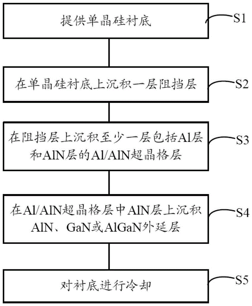
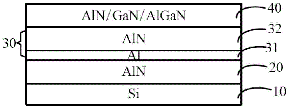
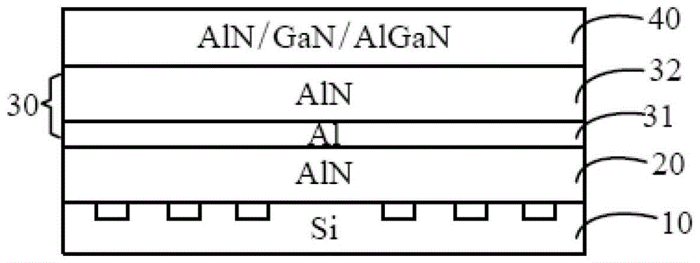
[0060] ginseng figure 1 As shown, the method for growing a nitride epitaxial layer on a silicon substrate of the present invention comprises:

[0061] S1. Provide a single crystal silicon substrate;

[0062] S2. Depositing a barrier layer on the single crystal silicon substrate;

[0063] S3, depositi...


PUM

PropertyMeasurementUnit
thicknessaaaaaaaaaa
melting pointaaaaaaaaaa

Abstract

The invention discloses a method for growing a nitride epitaxial layer on a silicon substrate, and a semiconductor device thereof. The method comprises the steps of providing a monocrystalline silicon substrate; depositing a barrier layer on the monocrystalline silicon substrate; depositing at least one Al / AlN superlattice layer containing an Al layer and an AlN layers on the barrier layer; depositing AlN, GaN or AlGaN epitaxial layers on the AlN layers of the Al / AlN superlattice layers, wherein in the process of depositing the AlN, GaN or AlGaN epitaxial layers, the Al layers of the Al / AlN superlattice layers are in melt state, so that stress between the Al layers and the adjacent barrier layer or AlN layers is released; and cooling the substrate after deposition of the epitaxial layers is finished. In the cooling process, the Al layers of the Al / AlN superlattice layers are cured again, and press stress is applied to the adjacent barrier layer or AlN layers adjacent to the Al layers. By melting the Al layers of the Al / AlN superlattice layers during the growth of the epitaxial layers, tension between the monocrystalline silicon substrate and the epitaxial layers can be effectively released; crack and dislocation phenomena caused by thermal mismatch and lattice mismatch are overcome; the crystalline quality of the epitaxial layers is increased; the performance of the device is enhanced; and the service life of the device is prolonged.

Description

technical field [0001] The invention relates to the field of semiconductor technology, in particular to a method for growing a nitride epitaxial layer on a silicon substrate and a semiconductor device thereof. Background technique [0002] Gallium nitride is considered to be the most important semiconductor material after silicon. GaN is a wide bandgap semiconductor material, its spectrum covers the entire visible light region, it can be made into blue and white light-emitting diodes for display, TV backlight and general lighting; it can be made into green / blue light-emitting diodes, Together with AlGaInP-based red light-emitting diodes, it is used for full-color display; it can also be made into ultraviolet lasers for data storage. In addition to excellent optical properties, gallium nitride also has excellent electrical properties: high electron mobility (~2000cm2 / Vs), high electron velocity (2.5E7cm / s), high critical electric field (3.5MV / cm), etc. Therefore, gallium ni...

Claims


Application Information

Patent Timeline
Patent Type & Authority Patents(China)
IPC IPC(8): H01L33/12H01L33/32H01L33/00
CPCH01L33/007H01L33/12H01L33/32
Inventor 马悦黄占超奚明
Owner DEPOSITION EQUIP & APPL SHANGHAI LTD
Features
  • R&D
  • Intellectual Property
  • Life Sciences
  • Materials
  • Tech Scout
  • Unparalleled Data Quality
  • Higher Quality Content
  • 60% Fewer Hallucinations
Learn More