

A high na projection objective lens
A technology of projection objective lens and object side, applied in the field of projection optics, can solve problems such as material type limitation, achieve the effect of simple and compact structure, reduce system length, and improve lithography resolution
- Summary
- Abstract
- Description
- Claims
- Application Information
AI Technical Summary
Problems solved by technology
Method used
Image

Examples
Embodiment Construction
[0030] In order to better illustrate the purpose and advantages of the present invention, the present invention will be further described below in conjunction with the accompanying drawings and specific embodiments.
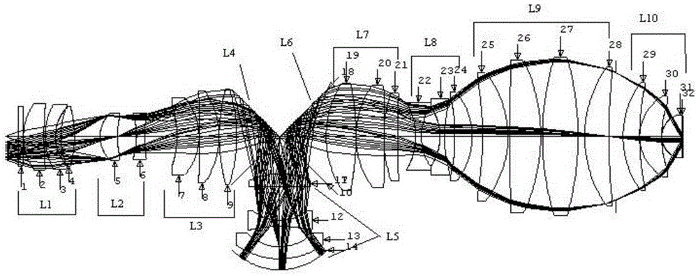
[0031] figure 1 It is a schematic diagram of the layout of the high NA projection objective lens of the present invention, 31 optical elements form the first unit L1, the second unit L2, the third unit L3, the fourth unit L4 and the fifth unit L5, the sixth unit L6, the seventh unit L7, An eighth unit L8, a ninth unit L9, and a tenth unit L10.
[0032] This high NA projection objective utilizes two flat mirrors to fold the optical system, effectively shortening the total system length. All the transmission mirrors in the present invention use fused silica material, and the refractive index of fused silica glass is 1.560491 at the central wavelength of 193 nm.
[0033] In order to meet the requirements of structural parameters and further improve the image quali...
PUM
| Property | Measurement | Unit |
|---|---|---|
| refractive index | aaaaa | aaaaa |
Abstract
Description
Claims
Application Information