Task mapping method for optimizing whole of on-chip network with acceleration nodes

An on-chip network and acceleration node technology, which is applied in inter-program communication, instruments, multi-programming devices, etc., can solve the problem of on-chip network bandwidth reduction and other issues

Inactive Publication Date: 2014-06-25
ZHEJIANG UNIV
View PDF4 Cites 7 Cited by
  • Summary
  • Abstract
  • Description
  • Claims
  • Application Information

AI Technical Summary

Problems solved by technology

When the scale of the network on chip is large, the links in the central area are more used to forward long-distance communication packets, which greatly reduces the bandwidth of the entire network on chip

Method used


Image

  • Task mapping method for optimizing whole of on-chip network with acceleration nodes
  • Task mapping method for optimizing whole of on-chip network with acceleration nodes
  • Task mapping method for optimizing whole of on-chip network with acceleration nodes

Examples


Embodiment Construction

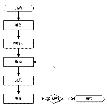
[0039] The present invention will be further analyzed below in conjunction with the accompanying drawings and specific embodiments.

[0040] Such as figure 1 Shown, the inventive method comprises the following steps:

[0041] Step (1). Preparation stage

[0042] 1.1 Accumulate the communication traffic of any two subtasks in advance to obtain the communication traffic between each pair of subtasks.

[0043] 1.2 Determine the range of feasible solutions for subtasks

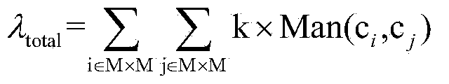
[0044] The present invention assumes that the amount of communication between m subtasks is 1, and then maps these subtasks on n processors; since the amount of communication between subtasks is set to 1, the overall calculation amount is very small , can be quickly solved by enumeration to obtain the region with the optimal feasible solution range of the subtask; the optimal region is the set of mapping layouts with the best fitness, as can be seen from formula (1):

[0045] Max { ...


PUM


Abstract

The invention discloses a task mapping method for optimizing the whole of an on-chip network with acceleration nodes. The task mapping method includes the steps of firstly determining a subtask feasible solution range and a fitness function, selecting feasible solution regions equal to subtasks in number from the subtask feasible solution range, carrying out random selection in the feasible solution regions to generate mapping layout sets, with the assigned number, of the initial subtasks, then carrying out selection and intersecting on the mapping layout sets of the initial subtasks, and exchanging the mapping positions of any two tasks in a mapping layout after intersected exchanging is carried out. According to the task mapping method, the inter-core communication cost and the task immigration cost after mapping are reduced, and the system performance is improved.

Description

technical field [0001] The invention relates to an on-chip multi-core interconnection network based on acceleration nodes, in particular to an optimized overall task mapping method for an on-chip network with acceleration nodes. Background technique [0002] With the rapid development of semiconductor technology and chip design technology, the number of transistors that can be integrated per unit area is increasing day by day, which greatly improves the performance of modern computers. However, with the increase in the complexity of processors, the cost of chip design and verification has also further increased, and the speed of increasing the frequency of a single processor has gradually slowed down in recent years, encountering a development bottleneck and unable to meet the increasing computer performance requirements. In order to solve this contradiction, the industry has gradually introduced multi-processor systems as an alternative to single-processor systems. A multi...

Claims


Application Information

Patent Timeline
Patent Type & Authority Applications(China)
IPC IPC(8): G06F9/54G06F15/173
Inventor 袁明敏邵景程孟静磊李颂元潘平傅唯威陈天洲刘莉施青松
Owner ZHEJIANG UNIV
Why Eureka
Try Eureka