This helps you quickly interpret patents by identifying the three key elements:
Problems solved by technology
Method used
Benefits of technology
Problems solved by technology
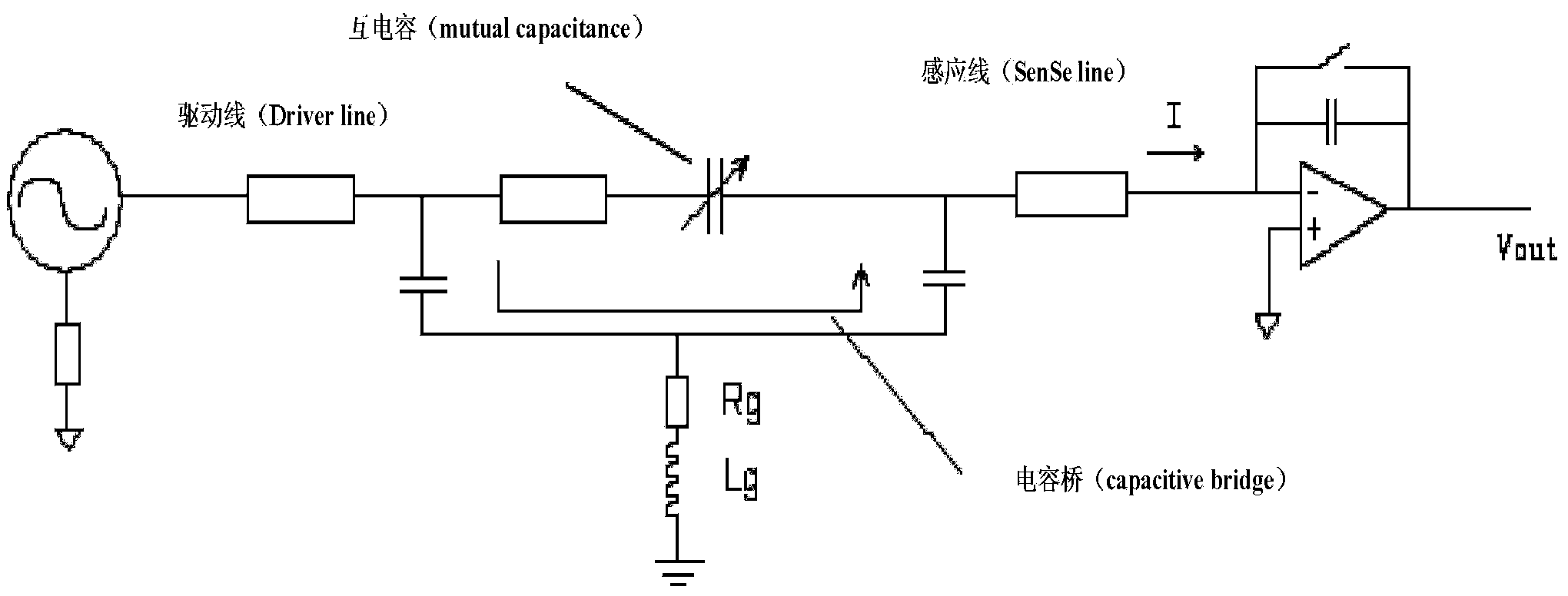
[0009] When the parasitic capacitance 105 is very large, the driving signal will be seriously deformed
In a touch-sensitive liquid crystal display device, due to the close distance between the touch layer and conductive layers such as pixel electrodes, data lines, and scan lines on the array substrate, the parasitic capacitance is large, which is not conducive to the detection of touch signals.
In addition, because the touch-sensitive liquid crystal display device needs to transmit light, as mentioned above, the touch layer must use a light-transmitting material such as indium tin oxide ITO film, and the resistivity of the ITO film is much higher than that of ordinary metals, so that The resistance of the touch layer is very large, which reduces the detection sensitivity of the touch layer and increases the load of the touch layer
Method used
Image
Click on the blue label to locate the original text in one second.
Reading with bidirectional positioning of images and text.
Examples
specific Embodiment 1
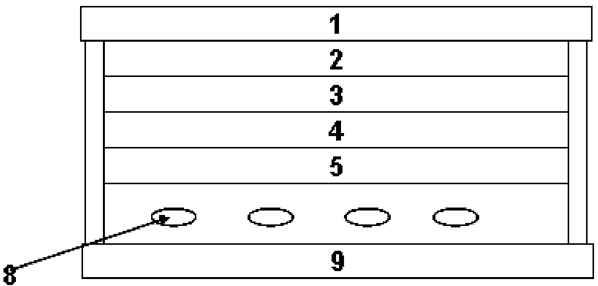
[0041] This embodiment provides a liquid crystal display device with a built-in touch screen, image 3 It is a schematic diagram of the structure of the liquid crystal display device. Such as image 3 As shown, the liquid crystal display device includes: a color filter substrate, an array substrate 9 and a liquid crystal layer 8 between the color filter substrate and the array substrate 9, and an organic layer 5, and the organic layer 5 serves as a protective layer. The color filter substrate includes a substrate 1, which is a glass substrate; a black matrix layer 2; a color filter layer 3; and a touch layer 4.
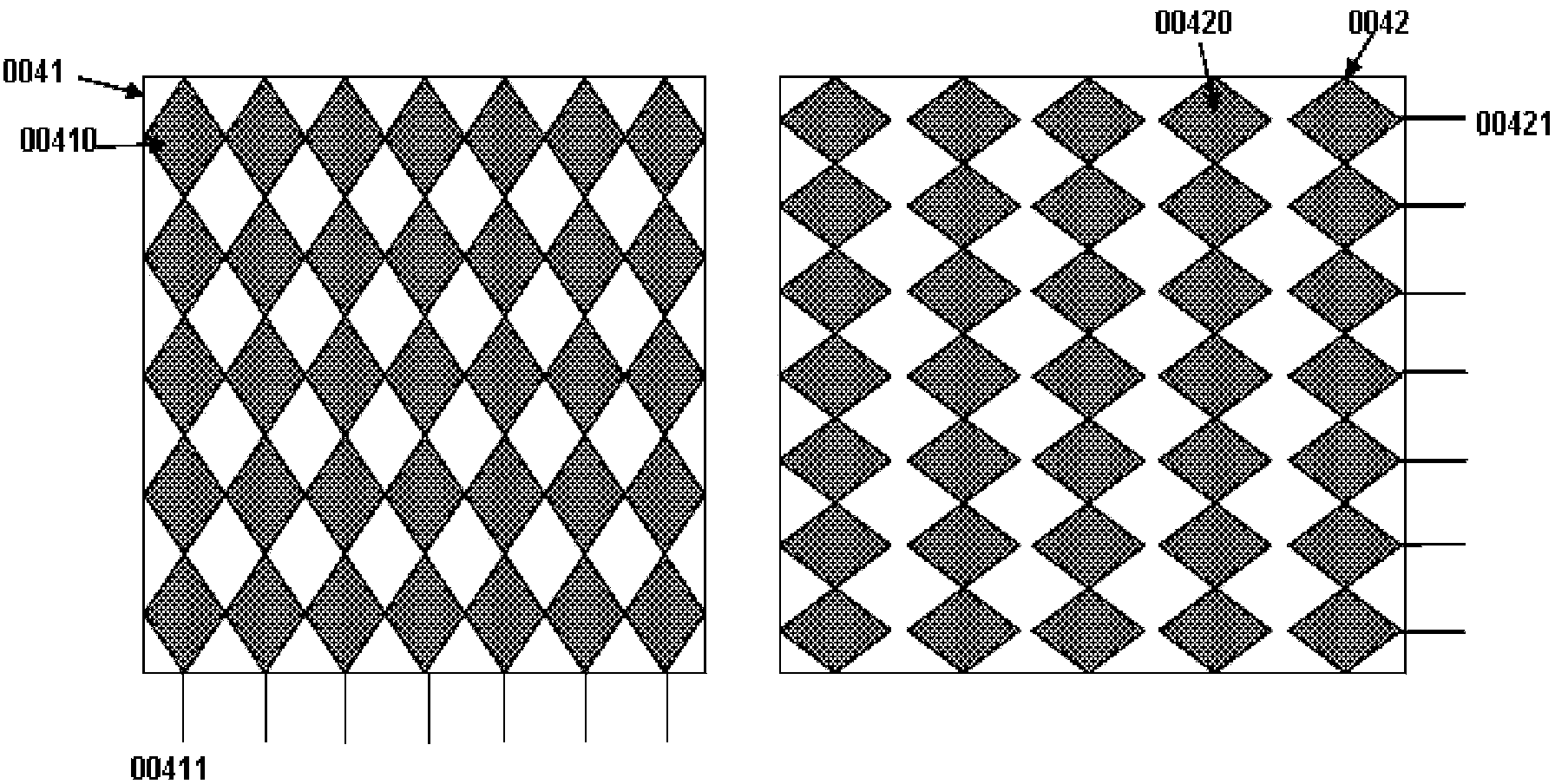
[0042] The top view of the black matrix layer is as follows Figure 4 As shown, the black matrix 2 is composed of criss-cross grids, and the material of the black matrix 2 is chromium, a commonly used black matrix material. Those skilled in the art can know that, Figure 4 It is only a partial illustration of the black matrix layer on the substrate, not all, and t...
specific Embodiment 2
[0054] In the in-cell touch display device provided by the specific embodiment 2, preferably, in the touch layer, the density of the metal grid decreases successively from adjacent sensing electrodes and driving electrodes to distant positions.
[0055] As a preferred embodiment, the attached Figure 8 is an exemplary structural diagram of a touch unit, as shown in the figure, the touch layer includes drive electrodes A1 and A2, sensing electrodes B1 and B2, and the drive electrodes A1 and A2, sensing electrodes B1 and B2 are the touch layer A pixel structure, and four electrodes are arranged adjacent to each other.
[0056] In the vicinity of the four electrodes, the metal grid density of each electrode is the largest. For example, the ratio of the metal grid density of the sensing electrode B1 to the density of the sub-pixel unit can be designed to be 1:1, that is, the sensing electrode A metal grid here in B1 corresponds to 1 / 3 pixel unit, that is, a sub-pixel unit, and a ...
PUM
Property
Measurement
Unit
width
aaaaa
aaaaa
Abstract
The invention discloses an embedded type touch control display device which comprises a color film substrate, a thin film transistor array substrate and a liquid crystal layer. The embedded type touch control display device is characterized in that the color film substrate comprises a latticed black matrix, a touch control layer and a color film layer; the touch control layer comprises a plurality of metal lattice electrodes arranged in a matrix, the metal lattice electrodes comprise a plurality of driving electrodes and a plurality of sensing electrodes, and in the light transmitting direction, projection of the metal lattice electrodes is located in the projection of the black matrix; the density of metal lattices close to adjacent sensing electrodes and driving electrodes is larger than the density of metal lattices away from the sensing electrodes and driving wires. The embedded type touch control display device can reduce resistance and stray capacitance in the structure, and a large-size embedded touch control structure is achieved.
Description
technical field [0001] The invention relates to the field of touch technology, in particular to a liquid crystal display device with a built-in touch screen. Background technique [0002] The touch screen is one of the important carriers for integrating input and output terminals. Demand for touchscreen displays has exploded in recent years with the introduction of a range of products, including the iPhone, a small, lightweight handheld device. Early touch display screens were realized by superimposing display screens and touch screens. That is, when preparing touch display screens, it is necessary to prepare display devices and touch screens separately, and then assemble the display devices and touch screens to form touch display devices. Higher, and the manufactured display screen is bulky, which does not meet the current demand for light weight and thinner display devices. [0003] The in-cell touch display screen has attracted people's attention because it integrates t...
Claims
Application Information
Patent Timeline
Application Date:The date an application was filed.
Publication Date:The date a patent or application was officially published.
First Publication Date:The earliest publication date of a patent with the same application number.
Issue Date:Publication date of the patent grant document.
PCT Entry Date:The Entry date of PCT National Phase.
Estimated Expiry Date:The statutory expiry date of a patent right according to the Patent Law, and it is the longest term of protection that the patent right can achieve without the termination of the patent right due to other reasons(Term extension factor has been taken into account ).
Invalid Date:Actual expiry date is based on effective date or publication date of legal transaction data of invalid patent.

