A two-dimensional phase change memory cell structure and its manufacturing method

A phase change memory and cell structure technology, applied in electrical components and other directions, can solve the problems of inability to realize energy consumption, low phase change memory cells, etc., and achieve the effects of ultra-low non-volatile information storage and ultra-low energy consumption

Active Publication Date: 2017-06-16
SHANGHAI XINCHU INTEGRATED CIRCUIT
View PDF6 Cites 0 Cited by
  • Summary
  • Abstract
  • Description
  • Claims
  • Application Information

AI Technical Summary

Problems solved by technology

[0007] In view of the above existing problems, the present invention proposes a two-dimensional phase-change memory unit and its manufacturing method to overcome the need to heat the phase-change material to a molten state in the phase-change memory technology in the prior art, which cannot achieve low energy consumption while having Problems with Higher Stability Phase Change Memory Cells

Method used


Image

  • A two-dimensional phase change memory cell structure and its manufacturing method
  • A two-dimensional phase change memory cell structure and its manufacturing method
  • A two-dimensional phase change memory cell structure and its manufacturing method

Examples


Embodiment 1

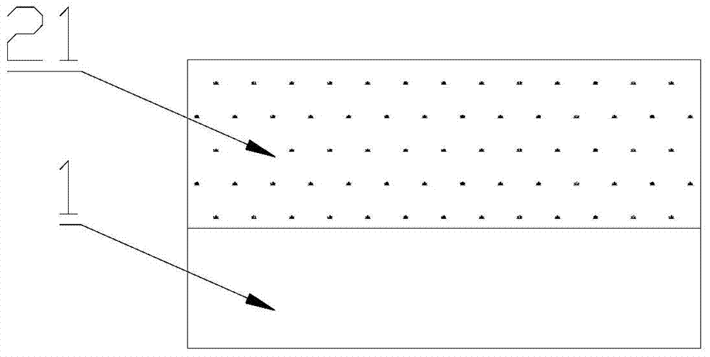
[0056] Figure 10 It is a structural schematic diagram of the phase change memory cell structure of this embodiment; as Figure 10 As shown, a phase-change memory cell structure includes: a substrate wafer 1; a first insulating layer 21 arranged above the substrate wafer 1, a lower electrode 3 is arranged in the first insulating layer 21, and a lower electrode 3 is placed under the lower electrode 3. The surface connection substrate wafer 1; the phase change structure 7 disposed above the first insulating layer 21 and the lower electrode 3; the second insulating layer 22 disposed above the phase change structure 7 and the first insulating layer 21, and the phase change structure 7 It includes a first phase-change auxiliary layer 71 , a phase-change material layer 72 and a second phase-change auxiliary layer 73 disposed above the bottom electrode 3 in sequence.

[0057] Among them, the substrate wafer 1 is a wafer prepared with a phase-change memory circuit, and the substrate ...

Embodiment 2

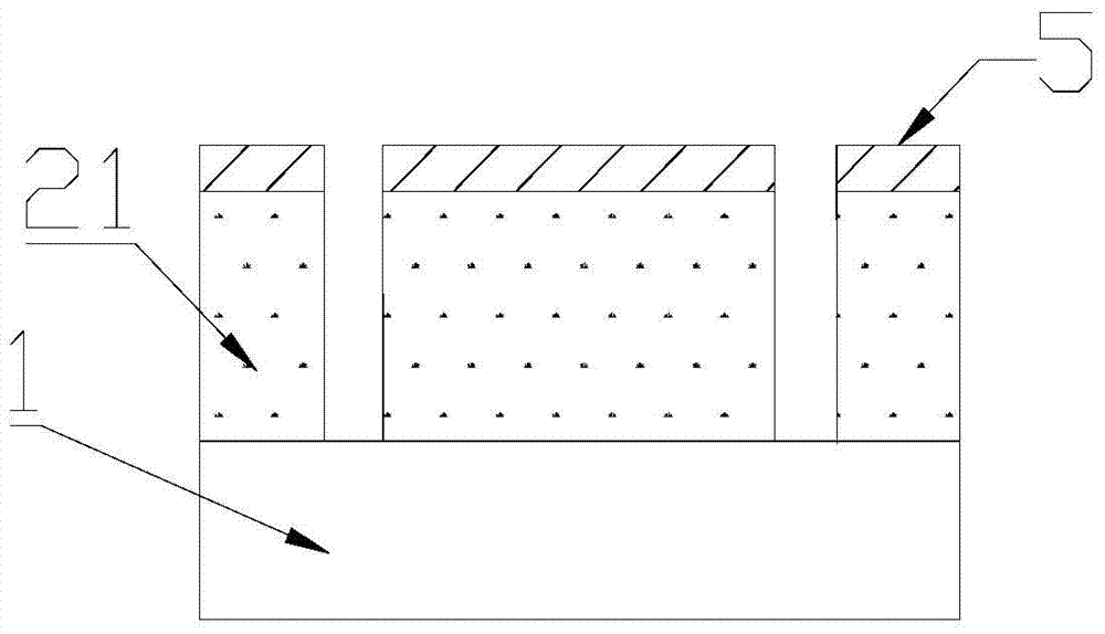
[0068] Figure 16 It is a structural schematic diagram of the phase change memory cell structure of this embodiment; as Figure 16 As shown, a phase change memory cell structure includes: a substrate wafer 1; a first insulating layer 21 arranged above the substrate wafer 1, and two lower electrodes 3 are arranged in the first insulating layer 21, and the lower electrode 3 The lower connection substrate wafer 1, the second insulating layer 22 disposed above the first insulating layer 21 and the lower electrode 3, the phase change structure 7 disposed in the second insulating layer 22, the phase change structure 7 An upper electrode 8 located above the lower electrode 3 and disposed above the phase change structure 7, wherein the phase change structure 7 includes a first phase change auxiliary layer, a phase change material layer and a second phase change layer sequentially disposed above the lower electrode 3 Change auxiliary layer.

[0069] The preparation method of the phas...

Embodiment 3

[0076] like Figure 16 As shown, the structure and preparation method of the present embodiment are similar to those of the second embodiment, the difference is that there is only one bottom electrode 3, and the phase change structure 7 is a square structure, which will not be repeated here.

[0077] In summary, in the above-mentioned embodiments, the phase-change material layer of the phase-change memory unit is sandwiched between two phase-change auxiliary layers, and the phase-change material layer is extremely thin, with a thickness of 0.1nm-10nm, within a few atomic layers. Between dozens of atomic layers, the phase-change material layer can achieve better lattice matching and auxiliary phase-change effect with the phase-change material. When the phase-change memory is working, under the action of electric and thermal fields, the phase-change material layer It does not need to reach a molten state, and can achieve low-energy non-volatile information storage through a phas...


PUM


Abstract

The invention discloses a two-dimensional phase-change memory unit structure, comprising: a substrate wafer; a first insulating layer arranged above the substrate wafer, a lower electrode is arranged in the first insulating layer, and the The lower surface of the lower electrode is connected to the substrate wafer; the second insulating layer is arranged on the first insulating layer and the lower electrode; it is arranged in the second insulating layer and covers the lower electrode A phase-change structure on the surface, and the phase-change structure includes a first phase-change auxiliary layer, a phase-change material layer and a second phase-change auxiliary layer sequentially arranged above the lower electrode. The present invention also provides a method for preparing the structure. The obtained two-dimensional phase-change memory unit structure has an extremely thin phase-change material layer. When working, the phase-change material layer does not need to reach a molten state under the action of an electric field and a thermal field. The resistance value of itself can be changed by exchanging atoms with the phase-change auxiliary layer or undergoing a phase change by itself, so as to realize non-volatile storage with low energy consumption.

Description

technical field [0001] The invention belongs to the technical field of semiconductors, and in particular relates to a two-dimensional phase-change memory unit structure and a manufacturing method thereof. Background technique [0002] Phase-change memory is an emerging non-volatile memory technology. It uses electrical pulses to rapidly transform phase-change materials in an ordered crystalline state (low resistance) and a disordered amorphous state (high resistance). Realize data storage. Phase-change memory has the characteristics of high speed, easier scaling to a smaller size, and high reliability, and it is likely to be a replacement for flash memory technology. At present, Micron Corporation of the United States has announced the mass production of 45nm phase-change memory. [0003] In order to achieve high-capacity, low power consumption, and fast phase-change memory, it is mainly achieved by reducing the volume of phase-change materials or reducing the size of heat...

Claims


Application Information

Patent Timeline
Patent Type & Authority Patents(China)
IPC IPC(8): H01L45/00
Inventor 亢勇陈邦明宋志棠
Owner SHANGHAI XINCHU INTEGRATED CIRCUIT
Why Eureka
Try Eureka