Semiconductor LED fluorescent packaging structure

A packaging structure and semiconductor technology, applied in semiconductor devices, electrical components, circuits, etc., can solve the problems of low efficiency and low efficiency of phosphors, and achieve the effects of improving light efficiency, reducing total reflection, and improving light output efficiency

Inactive Publication Date: 2014-07-09
河北豪莱装备科技有限公司
View PDF3 Cites 12 Cited by
  • Summary
  • Abstract
  • Description
  • Claims
  • Application Information

AI Technical Summary

Problems solved by technology

But stimulated LEDs are not as efficient as direct-emitting LEDs, partly because of inefficiencies in the process of phosphor absorption and re-emission

Method used


Image

  • Semiconductor LED fluorescent packaging structure
  • Semiconductor LED fluorescent packaging structure
  • Semiconductor LED fluorescent packaging structure

Examples


Embodiment 1

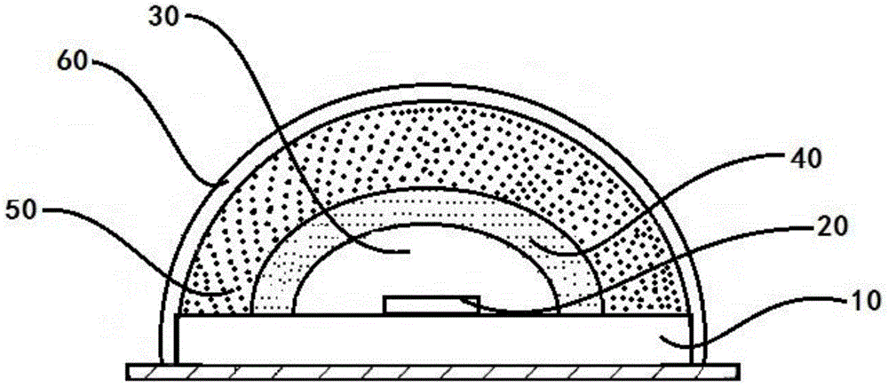
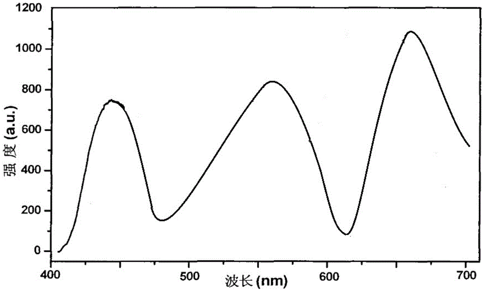
[0024] The phosphor contained in the first phosphor layer is Eu 26 al 12 Ca 2 MnO 60 . The phosphor contained in the second phosphor layer is Eu 15 Y 3 Ba 2 mn 1 o 30 . The average particle size of the phosphors is 4.2 μm. Using silicone resin as the transparent material, mixing the fluorescent powder with the transparent material, heating and curing to form the first fluorescent layer and the second fluorescent layer. The transparent resin of the first transparent diffuse reflection layer and the second transparent diffuse reflection layer is also selected from silicone resin. And use the blue LED package to form an attached figure 1 Package structure shown (without clear protective layer). After running the LED, measure its excitation spectrum, the result is as attached figure 2 shown.

[0025] transparent protective layer

[0026] In the present invention, the transparent protective layer can provide sufficient protection for the fluorescent layer, has good ...

Embodiment 2

[0028] The transparent protective layer described in this embodiment has a thickness of about 500 μm, which is composed of 21.0wt% MDI, 15.0wt% PEG1000, 4.0wt% terephthalic acid, 1.3wt% trimethylolpropane, 1.2wt% % of ethoxylated bisphenol F diacrylate, 2.0wt% of phenylthioethane ethyl acrylic acid, 1.5wt% of 2-undecylimidazole, 0.15wt% of defoamer BYK-052, 0.15wt% of Leveling agent BYK-307, 0.20wt% dibutyltin dilaurate, 5.5wt% nano-alumina, 8.0wt% isopropanol and the rest of butyl acetate at a stirring speed of 300-400 rpm, Stir for 30 minutes to obtain a prepolymer, and then apply and cure at 100° C. for 30 minutes.

Embodiment 3

[0030] The transparent protective layer described in this embodiment has a thickness of about 500 μm, which is composed of 20.5wt% MDI, 13.5wt% PEG1000, 3.5wt% terephthalic acid, 1.2wt% trimethylolpropane, 1.1wt% % of ethoxylated bisphenol F diacrylate, 2.2wt% of phenylthioethane ethyl acrylic acid, 1.8wt% of 2-undecylimidazole, 0.15wt% of defoamer BYK-052, 0.15wt% of Leveling agent BYK-307, 0.20wt% of dibutyltin dilaurate, 5.0wt% of nano-alumina, 7.5wt% of isopropanol and the rest of butyl acetate at a stirring speed of 300 to 400 rpm, Stir for 30 minutes to obtain a prepolymer, and then apply and cure at 100° C. for 30 minutes.


PUM


Abstract

The invention relates to a semiconductor LED fluorescent packaging structure. The semiconductor LED fluorescent packaging structure comprises a packaging substrate, wherein an LED element is attached to the surface of the packaging substrate and arranged in a transparent diffuse reflection layer on the packaging substrate, a first fluorescent layer is arranged on the outer surface of the transparent diffuse reflection layer, a second fluorescent layer is arranged on the outer surface of the first fluorescent layer, and a fluorescent protective layer is arranged on the outer surface of the second fluorescent layer. According to the semiconductor LED fluorescent packaging structure, yellow fluorescent powder and red fluorescent powder are arranged on the diffuse reflection layer, the problem of nonuniformity caused by mixed use of the yellow fluorescent powder and the red fluorescent powder is avoided, attenuation of the fluorescent powder is relieved, and the lighting effect of LEDs is improved. Meanwhile, total reflection in the packaging structure is reduced, and luminous efficiency is improved.

Description

technical field [0001] The invention belongs to the technical field of LED packaging, and more specifically, the invention relates to a semiconductor LED fluorescent packaging structure. Background technique [0002] Light-emitting diodes (LEDs) are solid-state light sources that work by combining electrons and holes at the p-semiconductor and n-semiconductor junction. White light sources utilizing light emitting diodes (LEDs) can have two basic configurations. In a basic structure of direct-emitting LEDs, white light is produced by directly emitting light from LEDs of different colors, such as by including red LEDs, combinations of green LEDs and blue LEDs, and combinations of blue LEDs and yellow LEDs white light. The other is the basic structure of the light source based on LED-stimulated phosphor. The light beam generated by a single LED is in a narrow wavelength range. The light beam is irradiated on the fluorescent material and excites the fluorescent material to gen...

Claims


Application Information

Patent Timeline
Patent Type & Authority Applications(China)
IPC IPC(8): H01L33/48H01L33/60H01L33/50
CPCH01L33/505H01L33/60
Inventor 高鞠
Owner 河北豪莱装备科技有限公司
Why Eureka
Try Eureka